DP8392CV National Semiconductor, DP8392CV Datasheet
DP8392CV
Specifications of DP8392CV
Available stocks


Related parts for DP8392CV

DP8392CV Summary of contents
Page 1
... DIP However the power isolation for the CTI is done by DC-to-DC conversion through a power transformer 1 0 System Diagram IEEE 802 3 Compatible Ethernet Cheapernet Local Area Network Chip Set C 1995 National Semiconductor Corporation TL F 11085 Features Compatible with Ethernet II IEEE 802 3 10Base5 and Y ...
Page 2
Block Diagram 3 0 Functional Description The CTI consists of four main logical blocks a) the Receiver - receives data from the coax and sends it to the DTE b) the Transmitter - accepts data from the DTE ...
Page 3
Functional Description 3 3 COLLISION FUNCTIONS The collision circuitry consists of two buffers two 4-pole Bessel low pass filters (section comparator a heart- beat generator a 10 MHz oscillator and a differential line driver Two ...
Page 4
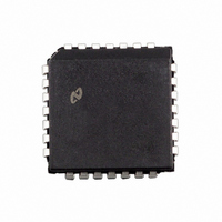
... Note pulse transformer L 100 H e Pulse Engineering (San Diego) Part No 64103 Valor Electronics (San Diego) Part No LT6003 or equivalent 5 0 Connection Diagrams Order Number DP8392CV See NS Package Number V28A FIGURE 4 Top View Order Number DP8392CN See NS Package Number N16E TL F 11085–6 ...
Page 5
Pin Descriptions 28-Pin PLCC 16-Pin DIP Name ...
Page 6
... EACH set of pins should be for applications with low transmitter duty cycle and for high transmit duty cycle applications Figure 7 illustrates a recommended component side layout for these planes FIGURE 7 Recommended Layout and Dissipation Planes for DP8392CV (Not to Scale ...
Page 7
... Conditions 12V Watts Supply Voltage (V EE See Section 5 Ambient Temperature If Military Aerospace specified devices are required 0 to 12V b please contact the National Semiconductor Sales 65 to 150 C b Office Distributors for availability and specifications 260 are measured after the pulse transformer except V ...
Page 8
DP8392C Switching Characteristics Symbol Parameter t Receiver startup delay (RXI to RX RON t Receiver propagation delay (RXI Differential outputs rise time ( Differential outputs fall time ( Receiver cable ...
Page 9
Timing and Load Diagrams FIGURE 8 Receiver Timing FIGURE 9 Transmitter Timing FIGURE 10 Collision Timing FIGURE 11 Heartbeat Timing 11085– 11085– 11085– 11085 – 10 ...
Page 10
Timing and Load Diagrams The 50 H inductance is for testing purposes Pulse transformers with higher inductances are recommended (see Figure 4 ) (Continued) FIGURE 12 Jabber Timing Receiver equalization (jitter correction Input jitter at ...
Page 11
Physical Dimensions inches (millimeters) Order Number DP8392CN or DP8392CN-1 Molded Dual-In-Line Package (N) NS Package Number N16E 11 ...
Page 12
... Physical Dimensions inches (millimeters) (Continued) Order Number DP8392CV or DP8392CV-1 LIFE SUPPORT POLICY NATIONAL’S PRODUCTS ARE NOT AUTHORIZED FOR USE AS CRITICAL COMPONENTS IN LIFE SUPPORT DEVICES OR SYSTEMS WITHOUT THE EXPRESS WRITTEN APPROVAL OF THE PRESIDENT OF NATIONAL SEMICONDUCTOR CORPORATION As used herein 1 Life support devices or systems are devices or ...