CYP15G0101DXB-BBXI Cypress Semiconductor Corp, CYP15G0101DXB-BBXI Datasheet - Page 22
CYP15G0101DXB-BBXI
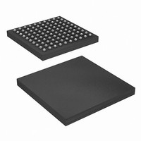
Manufacturer Part Number
CYP15G0101DXB-BBXI
Description
IC TXRX HOTLINK 100-LBGA
Manufacturer
Cypress Semiconductor Corp
Series
HOTlink II™r
Type
Transceiverr
Datasheet
1.CYP15G0101DXB-BBXC.pdf
(44 pages)
Specifications of CYP15G0101DXB-BBXI
Package / Case
100-LBGA
Protocol
Fibre Channel
Voltage - Supply
3.135 V ~ 3.465 V
Mounting Type
Surface Mount
Product
PHY
Data Rate
1500 MBd
Supply Voltage (max)
3.465 V
Supply Voltage (min)
3.135 V
Supply Current
0.51 A
Maximum Operating Temperature
+ 85 C
Minimum Operating Temperature
- 40 C
Mounting Style
SMD/SMT
Number Of Channels
1
Lead Free Status / RoHS Status
Lead free / RoHS Compliant
For Use With
CYP15G0101DX-EVAL - EVAL BRD FOR HOTLINK II
Number Of Drivers/receivers
-
Lead Free Status / Rohs Status
Lead free / RoHS Compliant
Available stocks
Company
Part Number
Manufacturer
Quantity
Price
Company:

Part Number:
CYP15G0101DXB-BBXI
Manufacturer:
SPANSION
Quantity:
1 200
Company:
Part Number:
CYP15G0101DXB-BBXI
Manufacturer:
Cypress Semiconductor Corp
Quantity:
10 000
Part Number:
CYP15G0101DXB-BBXI
Manufacturer:
CYPRESS/赛普拉斯
Quantity:
20 000


Parity Generation
In addition to the eleven data and status bits that are presented,
an RXOP parity output is also available. This allows the
CYP(V)(W)15G0101DXB to support ODD parity generation. To
handle
CYP(V)(W)15G0101DXB supports different forms of parity
generation (in addition to no parity). When the decoder is
enabled (DECMODE LOW), parity can be generated on
■
■
When the decoder is bypassed (DECMODE = LOW), parity can
be generated on
■
■
These modes differ in the number of bits which are included in
the parity calculation. For all cases, only ODD parity is provided
which ensures that at least one bit of the data bus is always a
logic-1. Those bits covered by parity generation are listed in
Table
Parity generation is enabled through the 3-level select PARCTL
input. When PARCTL = LOW, parity checking is disabled, and
the RXOP output is disabled (high Z).
Table 15. Output Register Parity Generation
When PARCTL = MID (open) and the decoder is enabled
(DECMODE LOW), ODD parity is generated for the received
and decoded character in the RXD[7:0] signals and is presented
on the RXOP output.
Document Number: 38-02031 Rev. *L
Notes
25. Receive path parity output driver (RXOP) is disabled (high Z) when PARCTL
26. When the decoder is bypassed (DECMODE = LOW) and BIST is not enabled (Receive BIST latch output is HIGH), RXST[2] is driven to a logic-0, except when the
RXST[2]
RXST[1]
RXST[0]
the RXD[7:0] character
the RXD[7:0] character and RXST[2:0] status.
the RXD[7:0] and RXST[1:0] bits
the RXD[7:0] and RXST[2:0] bits.
RXD[0]
RXD[1]
RXD[2]
RXD[3]
RXD[4]
RXD[5]
RXD[6]
RXD[7]
Signal
Name
character in the output buffer is a framing character.
15.
a
wide
LOW
Receive Parity Generate Mode (PARCTL)
[25]
range
DECMODE
= LOW
of
X
X
X
X
X
X
X
X
X
X
system
MID
DECMODE
LOW
environments,
X
X
X
X
X
X
X
X
HIGH
X
[26]
X
X
X
X
X
X
X
X
X
X
the
=
LOW.
When PARCTL = MID (open) and the decoder is bypassed
(DECMODE = LOW), ODD parity is generated for the received
and decoded character in the RXD[7:0] and RXST[1:0] bit
positions.
When PARCTL = HIGH, ODD parity is generated for the
TXD[7:0] and the RXST[2:0] status bits.
Receive Status Bits
When the 10B/8B decoder is enabled (DECMODE LOW),
each character presented at the output register includes three
associated status bits. These bits are used to identify
■
■
■
■
These conditions normally overlap; for example, a valid data
character received with incorrect running disparity is not reported
as a valid data character. It is instead reported as a decoder
violation of some specific type. This implies a hierarchy or priority
level to the various status bit combinations. The hierarchy and
value of each status is listed in
Within these status decodes, there are three forms of status
reporting. The two normal or data status reporting modes
(Type A and Type B) are selectable through the RXMODE input.
These status types allow compatibility with legacy systems, while
allowing full reporting in new systems. The third status type is
used for reporting receive BIST status and progress.
BIST Status State Machine
When the receive path is enabled to look for and compare the
received data stream with the BIST pattern, the RXST[2:0] bits
identify the present state of the BIST compare operation.
The BIST state machine has multiple states, as shown in
Figure 2 on page 24
an out-of-lock condition, the BIST state is forced to the
Start-of-BIST state, regardless of the present state of the BIST
state machine. If the number of detected errors ever exceeds the
number of valid matches by greater than 16, the state machine
is forced to the WAIT_FOR_BIST state where it monitors the
interface for the first character (D0.0) of the next BIST sequence.
Also, if the elasticity buffer ever hits and overflow/underflow
condition, the status is forced to the BIST_START until the buffer
is re-centered (approximately nine character periods).
To ensure compatibility between the source and destination
systems when operating in BIST, the sending and receiving ends
of the BIST sequence must use the same clock setup
(RXCKSEL = MID or RXCKSEL = LOW).
if the contents of the data bus are valid
the type of character present
the state of receive BIST operations (regardless of the state of
DECMODE)
character violations.
and
Table
16. When the receive PLL detects
Table
CYW15G0101DXB
CYP15G0101DXB
CYV15G0101DXB
16.
Page 22 of 44
[+] Feedback
Related parts for CYP15G0101DXB-BBXI
Image
Part Number
Description
Manufacturer
Datasheet
Request
R

Part Number:
Description:
Manufacturer:
Cypress Semiconductor Corp
Datasheet:
Part Number:
Description:
Manufacturer:
Cypress Semiconductor Corp
Datasheet:
Part Number:
Description:
Manufacturer:
Cypress Semiconductor Corp
Datasheet:
Part Number:
Description:
Manufacturer:
Cypress Semiconductor Corp
Datasheet:
Part Number:
Description:
Manufacturer:
Cypress Semiconductor Corp
Datasheet: