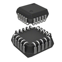
MIC59P60BV Micrel Inc, MIC59P60BV Datasheet - Page 4

MIC59P60BV
Manufacturer Part Number
MIC59P60BV
Description
IC DRVR LATCH 8BIT PAR IN 20PLCC
Manufacturer
Micrel Inc
Type
Driverr
Datasheet
1.MIC59P60YWM.pdf
(12 pages)
Specifications of MIC59P60BV
Number Of Drivers/receivers
8/0
Voltage - Supply
5V
Mounting Type
Surface Mount
Package / Case
20-LCC (J-Lead)
Lead Free Status / RoHS Status
Contains lead / RoHS non-compliant
Protocol
-
Available stocks
Company
Part Number
Manufacturer
Quantity
Price
Company:
Part Number:
MIC59P60BV
Manufacturer:
MICREL
Quantity:
231
MIC59P60
Timing Conditions
(T
A. Typical Data Active Time Before Clock Pulse (Data Set-Up Time) ........................................................................... 75 ns
B. Minimum Data Active Time After Clock Pulse (Data Hold Time) .............................................................................. 75 ns
C. Minimum Data Pulse Width ..................................................................................................................................... 150 ns
D. Minimum Clock Pulse Width .................................................................................................................................... 150 ns
E. Minimum Time Between Clock Activation and Strobe ............................................................................................. 300 ns
F. Minimum Strobe Pulse Width ................................................................................................................................... 100 ns
G. Typical Time Between Strobe Activation and Output Transition ............................................................................. 500 ns
SERIAL DATA present at the input is transferred to the shift register on the logic “0” to logic “1” transition of the CLOCK input
pulse. On succeeding CLOCK pulses, the registers shift data information towards the SERIAL DATA OUTPUT. The SERIAL
DATA must appear at the input prior to the rising edge of the CLOCK input waveform. Holding CLEAR high results in a data
logic "0" being clocked into the shift register, turning off respective channels.
Information present at any register is transferred to its respective latch when the STROBE is high (serial-to-parallel conversion).
The latches will continue to accept new data as long as the STROBE is held high. Applications where the latches are bypassed
(STROBE tied high) will require that the ENABLE input be high to prevent invalid output states.
When the ENABLE input is high, all of the output buffers are disabled (OFF) without affecting information stored in the latches
or shift register. With the ENABLE input low, the outputs are controlled by the state of the latches. A positive OE/RESET pulse
resets the FLAG and the output after a current shutdown fault. Over-temperature faults are not latched and require no reset
pulse.
MIC59P60 Truth Table
L = Low Logic Level
H = High Logic Level
X = Irrelevant
P = Present State
R = Previous State
O = Output OFF
MIC59P60
Serial
Input
Data
A
H
L
X
= +25 C, Logic Levels are V
OUTPUT
ENABLE
STROBE
DATA IN
CLOCK
OUT N
Clear Clock
Input Input
H
Shift Register Contents
I
R1
P
1
O
H
X
L
1
A
R2
R
R
P
C
I
O
X
2
B
1
1
2
DD
R
R
R
P
I
O ……
X ……
D
3
2
2
3
3
and V
E
……
……
……
……
……
SS,
R
R
R
P
I
O
X
8
7
7
8
8
V
DD
F
Output
G
Serial
Data
= 5V)
R
R
R
P
X
L
8
7
7
8
Strobe
Input
H
4
L
R
P
I
X
1
1
1
Latch Contents
R
P
I
X
2
2
2
R
P
I
X
3
3
3
……
……
……
……
R
P
I
X
8
8
8
Output
Enable I
H
L
P
H
1
1
Output Contents
I
P
2
H
2
August 2001
P
I
H …… H
3
3
……P
…… I
Micrel
8
8


