MIC59P60BV Micrel Inc, MIC59P60BV Datasheet - Page 2
MIC59P60BV
Manufacturer Part Number
MIC59P60BV
Description
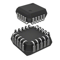
IC DRVR LATCH 8BIT PAR IN 20PLCC
Manufacturer
Micrel Inc
Type
Driverr
Datasheet
1.MIC59P60YWM.pdf
(12 pages)
Specifications of MIC59P60BV
Number Of Drivers/receivers
8/0
Voltage - Supply
5V
Mounting Type
Surface Mount
Package / Case
20-LCC (J-Lead)
Lead Free Status / RoHS Status
Contains lead / RoHS non-compliant
Protocol
-
Available stocks
Company
Part Number
Manufacturer
Quantity
Price
Company:

Part Number:
MIC59P60BV
Manufacturer:
MICREL
Quantity:
231


MIC59P60
PLCC Pin
Configuration
Typical Inputs
Typical Output Driver
Pin Description
MIC59P60
SERIAL DATA OUT
SERIAL DATA IN
DATA IN
SERIAL
CLOCK
12—19
STROBE
2,10
Pin
11
20
1
3
4
5
6
7
8
9
V DD
V SS
4
5
6
7
8
OUTPUT ENABLE/RESET
V
V
3
9
SS
MIC59P60BV
DD
SERIAL DATA OUT
SERIAL DATA IN
10
2
OUTPUT N
STROBE
CLOCK
CLEAR
Name
FLAG
V
V
V
11
STROBE
OUTPUT
ENABLE
K
1
EE
SS
DD
3K
12
20
SUB
V
EE
19
13
OUT
K
N
17
16
15
14
18
Description
Sets All Latches OFF (open).
Output Ground (Substrate). Most negative voltage in the system connects
here.
Serial Data Clock. A CLEAR must also be clocked into the latches.
Serial Data Input pin.
Logic reference (Ground) pin.
Logic Positive Supply voltage.
Serial Data Output pin. (Flow through).
Output Strobe pin. Loads output latches when High. A STROBE is needed
to CLEAR latches.
When Low, Outputs are active. When High, device is inactive and reset
from a fault condition. An under voltage condition emulates a high OE/
RESET input.
Transient suppression diode's cathode common pin.
Open Collector outputs 8 through 1.
Error Flag. Open-collector output is Low upon Overcurrent Fault or
Overtemperature fault. OUTPUT ENABLE/RESET must be pulled high to
reset the flag and fault condition.
OUT 2
OUT 3
OUT 4
OUT 5
OUT 6
V
V
SS
DD
2
Absolute Maximum Ratings
Output Voltage (V
Output Voltage (V
V
V
Emitter Supply Voltage (V
Input Voltage (V
Protected Current ............................................ 1.5A, Note 2
Power Dissipation (P
Operating Temperature (T
Storage Temperature (T
Junction Temperature (T
ESD ......................................................................... Note 3
Note 1:
Note 2:
Note 3:
DD
DD
Plastic DIP (N) ......................................................... 2.0W
PLCC (V) .................................................................1.4W
Wide SOIC (WM) .................................................... 1.2W
Plastic DIP (N), PLCC (V), SOIC (WM) .. –40 C to +85 C
with Reference to V
with Reference to V
Derate above T
Derate above T
Derate above T
For inductive load applications.
Each channel. V
inductance and resistance.
Devices are input-static protected but can be damaged by
extremetly high static charges.
IN
CE
CE(SUS)
) ............................... –0.3V to V
) .................................................... 80V
A
A
A
D
)
= +25 C ............................ 20mW/ C
= +25 C ............................ 14mW/ C
= +25 C ............................ 12mW/ C
EE
S
SS
EE
J
) ............................... 50V, Note 1
) ....................... –65 C to +150 C
connection must be designed to minimize
) ...................................... +150 C
EE
A
)
........................................... 15V
........................................... 25V
) ...................................... –20V
V
SS
= 0; T
August 2001
A
= 25 C
DD
Micrel
+0.3V
Related parts for MIC59P60BV
Image
Part Number
Description
Manufacturer
Datasheet
Request
R

Part Number:
Description:
Manufacturer:
Micrel Inc
Datasheet:
Part Number:
Description:
Manufacturer:
Micrel Inc
Datasheet:
Part Number:
Description:
Manufacturer:
Micrel Inc
Datasheet:
Part Number:
Description:
Manufacturer:
Micrel Inc
Datasheet:
Part Number:
Description:
Manufacturer:
Micrel Inc
Datasheet:
Part Number:
Description:
Manufacturer:
Micrel Inc
Datasheet:
Part Number:
Description:
Manufacturer:
Micrel Inc
Datasheet:
Part Number:
Description:
Manufacturer:
Micrel Inc
Datasheet:
Part Number:
Description:
Manufacturer:
Micrel Inc
Datasheet:
Part Number:
Description:
Manufacturer:
Micrel Inc
Datasheet:
Part Number:
Description:
Manufacturer:
Micrel Inc
Datasheet:
Part Number:
Description:
Manufacturer:
Micrel Inc
Datasheet:
Part Number:
Description:
Manufacturer:
Micrel Inc
Datasheet:
Part Number:
Description:
Manufacturer:
Micrel Inc
Datasheet: