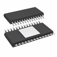
AD8392ARE Analog Devices Inc, AD8392ARE Datasheet - Page 12

AD8392ARE
Manufacturer Part Number
AD8392ARE
Description
IC LINE DRVR ADSL/ADSL2 28TSSOP
Manufacturer
Analog Devices Inc
Type
Driverr
Datasheet
1.AD8392AREZ-REEL.pdf
(16 pages)
Specifications of AD8392ARE
Number Of Drivers/receivers
2/0
Protocol
xDSL
Voltage - Supply
5 V ~ 24 V
Mounting Type
Surface Mount
Package / Case
28-TSSOP Exposed Pad, 28-eTSSOP, 28-HTSSOP
Power Supply Requirement
Single/Dual
Package Type
TSSOP EP
Slew Rate
900V/us
Pin Count
28
Lead Free Status / RoHS Status
Contains lead / RoHS non-compliant
Available stocks
Company
Part Number
Manufacturer
Quantity
Price
Company:
Part Number:
AD8392ARE
Manufacturer:
AD
Quantity:
5 510
Company:
Part Number:
AD8392ARE
Manufacturer:
TOS
Quantity:
5 510
Part Number:
AD8392AREZ
Manufacturer:
ADI/亚德诺
Quantity:
20 000
AD8392
APPLICATIONS
SUPPLIES, GROUNDING, AND LAYOUT
The AD8392 can be powered from either single or dual sup-
plies, with the total supply voltage ranging from 10 V to 24 V.
For optimum performance, a well regulated low ripple supply
should be used.
As with all high speed amplifiers, close attention should be paid
to supply decoupling, grounding, and overall board layout. Low
frequency supply decoupling should be provided with 10 µF
tantalum capacitors from each supply to ground. In addition, all
supply pins should be decoupled with 0.1 µF quality ceramic
chip capacitors placed as close as possible to the driver. An
internal low impedance ground plane should be used to provide
a common ground point for all driver and decoupling capacitor
ground requirements. Whenever possible, separate ground
planes should be used for analog and digital circuitry.
High speed layout techniques should be followed to minimize
parasitic capacitance around the inverting inputs. Some practi-
cal examples of these techniques are keeping feedback traces as
short as possible and clearing away ground plane in the area of
the inverting inputs. Input and output traces should be kept
short and as far apart from each other as practical to avoid
crosstalk. When used as a differential driver, all differential
signal traces should be kept as symmetrical as possible.
RESISTOR SELECTION
In current feedback amplifiers, selection of feedback and gain
resistors can impact harmonic distortion performance, band-
width, and gain flatness. Care should be exercised in the selec-
tion of these resistors so that optimum performance is achieved.
Table 5 shows some suggested resistor values for use in a variety
of gain settings. These values are suggested as a good starting
point when designing for any application.
Table 5. Resistor Selection Guide
Gain
1
2
5
10
POWER MANAGEMENT
The AD8392 can be configured in any of three active bias states
as well as a shutdown state via the use of two sets of digitally
programmable logic pins. Pins PD(0, 1) 1, 2 control Amplifiers
1 and 2, while PD(0, 1) 3, 4 control Amplifiers 3 and 4. These
pins can be controlled directly with either 3.3 V or 5 V CMOS
logic by using the GND pins as a reference. If left unconnected,
the PD pins float low, placing the amplifier in the full bias
mode. Refer to the Specifications for the per amplifier quiescent
current for each of the available bias states.
R
2.0k
1.5k
1.0k
750
F
R
Open
1.5k
249
82.5
G
Rev. A | Page 12 of 16
The AD8392 exhibits low output impedance for the three active
states. However, the output impedance in the shutdown state
(PD1, 0 = 1, 1) is undefined.
DRIVING CAPACITIVE LOADS
When driving a capacitive load, most op amps exhibit peaking
in their frequency response. In general, to minimize peaking or
to ensure device stability for larger values of capacitive loads, a
small series resistor can be added between the op amp output
and the load capacitor. Figure 34 shows the frequency response
of the AD8392 for various capacitive loads without any series
resistance. In this condition, the maximum recommended
capacitive load is around 20 pF. As shown in Figure 35, the
addition of a 5.1 Ω series resistor limits peaking to approxi-
mately 3 dB when driving capacitive loads up to 100 pF.
–10
–15
–10
–15
20
15
10
–5
20
15
10
–5
5
0
5
0
0.1
0.1
Figure 34. AD8392 Capacitive Load Frequency Response
Figure 35. AD8392 Capacitive Load Frequency Response
V
V
IN
IN
499Ω
499Ω
50Ω
50Ω
1
1
without Series Resistance
2kΩ
2kΩ
with Series Resistance
FREQUENCY (MHz)
FREQUENCY (MHz)
C
L
5.1Ω
C
10
L
10
1kΩ
1kΩ
100pF
100
100
47pF
22pF
20pF
15pF
10pF
1000
1000


