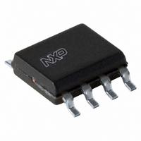
PCA82C251T/N3,112 NXP Semiconductors, PCA82C251T/N3,112 Datasheet - Page 3

PCA82C251T/N3,112
Manufacturer Part Number
PCA82C251T/N3,112
Description
IC CAN TRANSCEIVER 5V HS 8-SOIC
Manufacturer
NXP Semiconductors
Type
Transceiverr
Datasheet
1.PCA82C251N3112.pdf
(16 pages)
Specifications of PCA82C251T/N3,112
Package / Case
8-SOIC (3.9mm Width)
Number Of Drivers/receivers
1/1
Protocol
CAN
Voltage - Supply
4.5 V ~ 5.5 V
Mounting Type
Surface Mount
Product
Controller Area Network (CAN)
Number Of Transceivers
1
Data Rate
1 MBd
Supply Voltage (max)
5.5 V
Supply Voltage (min)
4.5 V
Supply Current (max)
275 uA
Maximum Operating Temperature
+ 125 C
Minimum Operating Temperature
- 40 C
Mounting Style
SMD/SMT
Interface
CAN
Lead Free Status / RoHS Status
Lead free / RoHS Compliant
Other names
568-5024
935196020112
PCA82C251T/N3,112
PCA82C251TD
PCA82C251TD
935196020112
PCA82C251T/N3,112
PCA82C251TD
PCA82C251TD
NXP Semiconductors
8. Functional description
PCA82C251_4
Product data sheet
7.2 Pin description
Table 3.
The PCA82C251 is the interface between a CAN protocol controller and the physical bus.
It is primarily intended for applications up to 1 MBd in trucks and buses. The device
provides differential transmit capability to the bus and differential receive capability to the
CAN controller. It is fully compatible with the “ISO 11898-24 V” standard.
A current-limiting circuit protects the transmitter output stage against short-circuits to
positive and negative battery voltage. Although power dissipation will increase as a result
of a short circuit fault condition, this feature will prevent destruction of the transmitter
output stage.
If the junction temperature exceeds approximately 160 °C, the limiting current of both
transmitter outputs is decreased. Because the transmitter is responsible for most of the
power dissipated, this will result in reduced power dissipation and hence a lower chip
temperature. All other parts of the IC will remain operational. The thermal protection is
needed, in particular, when a bus line is short-circuited.
The CANH and CANL lines are also protected against electrical transients which may
occur in an automotive environment.
Pin 8 (Rs) allows three different modes of operation to be selected: High-speed, Slope
control and Standby.
For high-speed operation, the transmitter output transistors are simply switched on and off
as fast as possible. In this mode, no measures are taken to limit the rise and fall slopes. A
shielded cable is recommended to avoid RFI problems. High-speed mode is selected by
connecting pin 8 to ground.
Slope control mode allows the use of an unshielded twisted pair or a parallel pair of wires
as bus lines. To reduce RFI, the rise and fall slopes should be limited. The rise and fall
slopes can be programmed with a resistor connected from pin 8 to ground. The slope is
proportional to the current output at pin 8.
If a HIGH level is applied to pin 8, the circuit enters a low-current Standby mode. In this
mode, the transmitter is switched off and the receiver is switched to a low current. If
dominant bits are detected (differential bus voltage >0.9 V), RXD will be switched to a
Symbol
TXD
GND
V
RXD
V
CANL
CANH
Rs
CC
ref
Pin description
Pin
1
2
3
4
5
6
7
8
Rev. 04 — 28 January 2010
Description
transmit data input
ground
supply voltage
receive data output
reference voltage output
LOW-level CAN voltage input/output
HIGH-level CAN voltage input/output
slope resistor input
CAN transceiver for 24 V systems
PCA82C251
© NXP B.V. 2010. All rights reserved.
3 of 16


