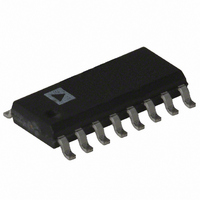
AD808-622BRRL7 Analog Devices Inc, AD808-622BRRL7 Datasheet - Page 9

AD808-622BRRL7
Manufacturer Part Number
AD808-622BRRL7
Description
IC FIBER OPTIC RCVR 16-SOIC
Manufacturer
Analog Devices Inc
Type
Receiverr
Datasheet
1.AD808-622BRZRL7.pdf
(12 pages)
Specifications of AD808-622BRRL7
Rohs Status
RoHS non-compliant
Voltage - Supply
4.5 V ~ 5.5 V
Mounting Type
Surface Mount
Package / Case
16-SOIC (3.9mm Width)
Operating Temperature (max)
85C
Operating Temperature (min)
-40C
Package Type
SOIC N
Pin Count
16
Mounting
Surface Mount
Number Of Drivers/receivers
-
Protocol
-
Lead Free Status / RoHS Status
Not Compliant
REV. 0
USING THE AD808
Acquisition Time
This is the transient time, measured in bit periods, that required
for the AD808 to lock onto the input data from its free running
state.
Ground Planes
The use of one ground plane for connections to both analog and
digital grounds is recommended.
Power Supply Connections
The use of a 10 F capacitor between V
mended. The +5 V power supply connection to V
carefully isolated. The V
provide the CLKOUT and DATAOUT signals.
Use a 0.1 F decoupling capacitor between IC power supply
input and ground. This decoupling capacitor should be posi-
tioned as closed to the IC as possible. Refer to the schematic in
Figure 15 for advised connections.
Transmission Lines
Use 50
DATAOUT signals.
Terminations
Use metal, thick-film, 1% termination resistors for PIN, NIN,
CLKOUT, and DATAOUT signals. These termination resistors
must be positioned as close to the IC as possible.
Use individual connections, not daisy chained, for connections
from the +5 V to load resistors for PIN, NIN, CLKOUT, and
DATAOUT signals.
transmission line for PIN, NIN, CLKOUT, and
CC2
pin is used inside the AD808 to
CC
and ground is recom-
CC2
should be
–9–
Loop Damping Capacitor, C
A ceramic capacitor may be used for the loop damping capaci-
tor. Using a 0.47 F, 20% capacitor provides < 0.1 dB jitter
peaking.
AD808 Output Squelch Circuit
A simple P-channel FET circuit can be used in series with the
Output Signal ECL Supply (V
data outputs when SDOUT indicates a loss of signal (Figure
16). The V
of 4 ECL loads, plus 16 mA for all 4 ECL output stages). This
means that selection of a FET with ON RESISTANCE of
0.5
only 36 mV.
will affect the common mode of the ECL outputs by
CC2
5V
BYPASS
Figure 16. Squelch Circuit Schematic
CAP
supply pin draws roughly 72 mA (14 mA for each
P_FET
TO V
1
2
3
4
5
6
7
8
CC1
DATAOUTN
DATAOUTP
V
CLKOUTN
CLKOUTP
V
CF1
CF2
CC2
CC1
D
CC2
, AV
, Pin 3) to squelch clock and
CC
AD808
, AV
CC2
THRADJ
SDOUT
AV
AV
AV
V
CC2
PIN
NIN
CC1
EE
EE
16
15
14
13
12
10
11
9
AD808


