AD808-622BRRL7 Analog Devices Inc, AD808-622BRRL7 Datasheet
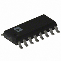
IC FIBER OPTIC RCVR 16-SOIC

AD808-622BRRL7

Manufacturer Part Number
AD808-622BRRL7
Description
IC FIBER OPTIC RCVR 16-SOIC
Manufacturer
Analog Devices Inc
Type
Receiverr
Datasheet

Specifications of AD808-622BRRL7

Rohs Status
RoHS non-compliant
Voltage - Supply
4.5 V ~ 5.5 V
Mounting Type
Surface Mount
Package / Case
16-SOIC (3.9mm Width)
Operating Temperature (max)
85C
Operating Temperature (min)
-40C
Package Type
SOIC N
Pin Count
16
Mounting
Surface Mount
Number Of Drivers/receivers
-
Protocol
-
Lead Free Status / RoHS Status
Not Compliant
a
PRODUCT DESCRIPTION
The AD808 provides the receiver functions of data quantiza-
tion, signal level detect, clock recovery and data retiming for
622 Mbps NRZ data. The device, together with a PIN
diode/preamplifier combination, can be used for a highly inte-
grated, low cost, low power SONET OC-12 or SDH STM-4
fiber optic receiver.
The receiver front end signal level detect circuit indicates when
the input signal level has fallen below a user adjustable thresh-
old. The threshold is set with a single external resistor. The
signal level detect circuit 3 dB optical hysteresis prevents chatter
at the signal level detect output.
The PLL has a factory trimmed VCO center frequency and a
frequency acquisition control loop that combine to guarantee
REV. 0
Information furnished by Analog Devices is believed to be accurate and
reliable. However, no responsibility is assumed by Analog Devices for its
use, nor for any infringements of patents or other rights of third parties
which may result from its use. No license is granted by implication or
otherwise under any patent or patent rights of Analog Devices.
FEATURES
Meets CCITT G.958 Requirements
Meets Bellcore TR-NWT-000253 Requirements for OC-12
Output Jitter: 2.5 Degrees RMS
622 Mbps Clock Recovery and Data Retiming
Accepts NRZ Data, No Preamble Required
Phase-Locked Loop Type Clock Recovery—
Quantizer Sensitivity: 4 mV
Level Detect Range: 10 mV to 40 mV, Programmable
Single Supply Operation: +5 V or –5.2 V
Low Power: 400 mW
10 KH ECL/PECL Compatible Output
Package: 16-Lead Narrow 150 mil SOIC
for STM-4 Regenerator—Type A
No Crystal Required
THRADJ
NIN
PIN
COMPARATOR/
DETECT
BUFFER
LEVEL
QUANTIZER
DETECTOR
SIGNAL
LEVEL
FUNCTIONAL BLOCK DIAGRAM
Fiber Optic Receiver with Quantizer and
SDOUT
F
DET
DET
AD808
Clock Recovery and Data Retiming
PHASE-LOCKED LOOP
COMPENSATING
frequency acquisition without false lock. This eliminates a reli-
ance on external components such as a crystal or a SAW filter,
to aid frequency acquisition.
The AD808 acquires frequency and phase lock on input data
using two control loops that work without requiring external
control. The frequency acquisition control loop initially acquires
the frequency of the input data, acquiring frequency lock on
random or scrambled data without the need for a preamble. At
frequency lock, the frequency error is zero and the frequency
detector has no further effect. The phase acquisition control
loop then works to ensure that the output phase tracks the input
phase. A patented phase detector has virtually eliminated pat-
tern jitter throughout the AD808.
The device VCO uses a ring oscillator architecture and patented
low noise design techniques. Jitter is 2.5 degrees rms. This low
jitter results from using a fully differential signal architecture,
Power Supply Rejection Ratio circuitry and a dielectrically
isolated process that provides immunity from extraneous signals
on the IC. The device can withstand hundreds of millivolts of
power supply noise without an effect on jitter performance.
The user sets the jitter peaking and acquisition time of the PLL
by choosing a damping factor capacitor whose value determines
loop damping. CCITT G.958 Type A jitter transfer require-
ments can easily be met with a damping factor of 5 or greater.
Device design guarantees that the clock output frequency will
drift by less than 20% in the absence of input data transitions.
Shorting the damping factor capacitor, C
output frequency to the VCO center frequency.
The AD808 consumes 400 mW and operates from a single
power supply at either +5 V or –5.2 V.
One Technology Way, P.O. Box 9106, Norwood, MA 02062-9106, U.S.A.
Tel: 781/329-4700
Fax: 781/326-8703
ZERO
RETIMING
DEVICE
CF1 CF2
FILTER
LOOP
World Wide Web Site: http://www.analog.com
VCO
CLKOUTP
CLKOUTN
DATAOUTP
DATAOUTN
© Analog Devices, Inc., 1998
D
, brings the clock
AD808

Related parts for AD808-622BRRL7

AD808-622BRRL7 Summary of contents

Page 1

... Device design guarantees that the clock output frequency will drift by less than 20% in the absence of input data transitions. Shorting the damping factor capacitor, C output frequency to the VCO center frequency. The AD808 consumes 400 mW and operates from a single power supply at either + –5.2 V. FUNCTIONAL BLOCK DIAGRAM QUANTIZER ...

Page 2

... AD808–SPECIFICATIONS Parameter QUANTIZER–DC CHARACTERISTICS Input Voltage Range Input Sensitivity, V SENSE Input Overdrive Input Offset Voltage Input Current Input RMS Noise Input Peak-to-Peak Noise QUANTIZER–AC CHARACTERISTICS Upper –3 dB Bandwidth Input Resistance Input Capacitance Pulsewidth Distortion LEVEL DETECT Level Detect Range ...

Page 3

... RECOVERED CLOCK SKEW Figure 2. Setup and Hold Time Model AD808-622BR AD808-622BRRL7 AD808-622BRRL CAUTION ESD (electrostatic discharge) sensitive device. Electrostatic charges as high as 4000 V readily accumulate on the human body and test equipment and can discharge without detection. Although the AD808 features proprietary ESD protection circuitry, permanent damage may occur on devices subjected to high energy electrostatic discharges ...

Page 4

... This is the frequency at which the VCO will oscillate with the loop damping capacitor shorted. D Tracking Range This is the range of input data rates over which the AD808 will remain in lock. Capture Range This is the range of input data rates over which the AD808 will acquire lock. ...

Page 5

... PIN (Pin 13) and NIN (Pin 12) as shown in Figure 4a. This allows very simple capacitive coupling of the signal from the preamp in the AD808 as shown in Figure 3. The internal common-mode potential is a diode drop (ap- proximately 0.8 V) below the positive supply as shown in Figure 4a ...

Page 6

... AD808–Typical Performance Characteristics 90000 80000 70000 60000 50000 40000 30000 20000 10000 SIGNAL DETECT VOLTAGE – mV Figure 5. Signal Detect Voltage vs. R 8.0 7 7.0 6 6.0 5.5 5 4.5 4.0 –40 – TEMPERATURE – C Figure 6. Signal Detect Hysteresis vs. Temperature STATIC PHASE – Degrees Figure 7. Histogram of Static Phase – ...

Page 7

... Traditionally, high speed comparators are plagued by crosstalk between outputs and inputs, often resulting in oscillations when the input signal approaches 10 mV. The AD808 quantizer toggles (4.0 mV sensitivity) at the input without making bit errors. When the input signal is low- ered below 2 mV, circuit performance is dominated by input noise, and not crosstalk ...

Page 8

... AD808 Center Frequency Clamp (Figure 13) An N-channel FET circuit can be used to bring the AD808 VCO center frequency to within 10% of 622 MHz when SDOUT indicates a Loss of Signal (LOS). This effectively re- duces the frequency acquisition time by reducing the frequency error between the VCO frequency and the input data frequency at clamp release. The N-FET can have “ ...

Page 9

... USING THE AD808 Acquisition Time This is the transient time, measured in bit periods, that required for the AD808 to lock onto the input data from its free running state. Ground Planes The use of one ground plane for connections to both analog and digital grounds is recommended. ...

Page 10

... AD808 0.1574 (4.00) 0.1497 (3.80) 0.0098 (0.25) 0.0040 (0.10) OUTLINE DIMENSIONS Dimensions shown in inches and (mm). 16-Lead Small Outline IC Package (R-16A) 0.3937 (10.00) 0.3859 (9.80 0.2440 (6.20 0.2284 (5.80) PIN 1 0.0688 (1.75) 0.0196 (0.50) 0.0532 (1.35) 0.0099 (0.25) 8 0.0500 0.0192 (0.49) 0 SEATING ...

Page 11

–11– ...

Page 12

–12– ...

Related keywords