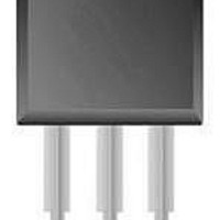
BUK9520-55 NXP Semiconductors, BUK9520-55 Datasheet - Page 2

BUK9520-55
Manufacturer Part Number
BUK9520-55
Description
MOSFET Power RAIL PWR-MOS
Manufacturer
NXP Semiconductors
Specifications of BUK9520-55
Configuration
Single
Transistor Polarity
N-Channel
Resistance Drain-source Rds (on)
0.02 Ohms
Drain-source Breakdown Voltage
55 V
Gate-source Breakdown Voltage
+/- 10 V
Continuous Drain Current
52 A
Power Dissipation
116 W
Maximum Operating Temperature
+ 175 C
Mounting Style
Through Hole
Package / Case
TO-220AB
Minimum Operating Temperature
- 55 C
Lead Free Status / Rohs Status
Details
Other names
BUK9520-55,127
Available stocks
Company
Part Number
Manufacturer
Quantity
Price
Company:
Part Number:
BUK9520-55
Manufacturer:
PHILIPS
Quantity:
5 000
Company:
Part Number:
BUK9520-55
Manufacturer:
NXP
Quantity:
12 500
Part Number:
BUK9520-55
Manufacturer:
PHILIPS/飞利浦
Quantity:
20 000
Company:
Part Number:
BUK9520-55A
Manufacturer:
NXP
Quantity:
36 000
Company:
Part Number:
BUK9520-55A
Manufacturer:
NXP
Quantity:
12 500
Philips Semiconductors
STATIC CHARACTERISTICS
T
DYNAMIC CHARACTERISTICS
T
REVERSE DIODE LIMITING VALUES AND CHARACTERISTICS
T
April 1998
TrenchMOS
Logic level FET
j
SYMBOL PARAMETER
V
V
I
I
R
mb
SYMBOL PARAMETER
g
C
C
C
t
t
t
t
L
L
L
j
SYMBOL PARAMETER
I
I
V
t
Q
= 25˚C unless otherwise specified
DSS
GSS
d on
r
d off
f
DR
DRM
rr
= 25˚C unless otherwise specified
V
fs
d
d
s
(BR)DSS
GS(TO)
SD
DS(ON)
iss
oss
rss
rr
= 25˚C unless otherwise specified
(BR)GSS
Drain-source breakdown
voltage
Gate threshold voltage
Zero gate voltage drain current
Gate source leakage current
Gate-source breakdown
voltage
Drain-source on-state
resistance
Forward transconductance
Input capacitance
Output capacitance
Feedback capacitance
Turn-on delay time
Turn-on rise time
Turn-off delay time
Turn-off fall time
Internal drain inductance
Internal drain inductance
Internal source inductance
Continuous reverse drain
current
Pulsed reverse drain current
Diode forward voltage
Reverse recovery time
Reverse recovery charge
transistor
CONDITIONS
V
V
V
V
I
V
CONDITIONS
V
V
V
V
Resistive load
Measured from contact screw on
tab to centre of die
Measured from drain lead 6 mm
from package to centre of die
Measured from source lead 6 mm
from package to source bond pad
CONDITIONS
I
I
I
V
G
F
F
F
GS
DS
DS
GS
GS
DS
GS
DD
GS
GS
= 25 A; V
= 40 A; V
= 40 A; -dI
= 1 mA;
= 0 V; I
= V
= 55 V; V
= 5 V; V
= 5 V; I
= 25 V; I
= 0 V; V
= 30 V; I
= 5 V; R
= -10 V; V
GS
; I
2
D
D
D
GS
GS
DS
G
D
D
F
= 0.25 mA;
= 1 mA
= 25 A
GS
DS
/dt = 100 A/ s;
= 10
= 25 A
= 25 A;
= 0 V
= 0 V
R
= 25 V; f = 1 MHz
= 30 V
= 0 V;
= 0 V
T
T
T
T
T
T
j
j
j
j
j
j
= 175˚C
= 175˚C
= 175˚C
= 175˚C
= -55˚C
= -55˚C
MIN.
MIN.
MIN.
0.5
55
50
10
20
1
-
-
-
-
-
-
-
-
-
-
-
-
-
-
-
-
-
-
-
-
-
-
-
TYP.
TYP.
1800
TYP.
0.05
0.02
0.95
0.15
350
170
110
1.5
3.5
4.5
7.5
1.0
15
28
95
70
47
-
-
-
-
-
-
-
-
-
-
Product specification
BUK9520-55
MAX.
MAX.
MAX.
2400
500
420
235
160
135
208
2.3
1.2
10
10
20
42
40
90
52
2
1
-
-
-
-
-
-
-
-
-
-
-
Rev 1.100
UNIT
UNIT
UNIT
m
m
nH
nH
nH
pF
pF
pF
ns
ns
ns
ns
ns
V
V
V
V
V
S
A
A
V
C
A
A
A
A


