DS21448 Maxim Integrated Products, DS21448 Datasheet
DS21448
Specifications of DS21448
Available stocks


Related parts for DS21448

DS21448 Summary of contents
Page 1
... GENERAL DESCRIPTION The DS21448 is a quad-port line interface unit (LIU) for short-haul and long-haul applications. It incorporates four independent transmitters and four independent receivers in a single 144-pin PBGA or 128-pin LQFP package. The generate the necessary G.703 E1 waveshapes in 75Ω or 120Ω applications and the DSX-1 or CSU line build-outs of 0dB, -7 ...
Page 2
... BLOCK DIAGRAMS ........................................................................................................................ 5 2. PIN DESCRIPTION .......................................................................................................................... 7 3. DETAILED DESCRIPTION ............................................................................................................ 13 3.1 DS21448 DS21Q348 D AND 4. PORT OPERATION ....................................................................................................................... 14 4 ......................................................................................................................... 14 ARDWARE ODE 4 ERIAL ORT PERATION 4 ARALLEL ORT PERATION 4.3.1 Device Power-Up and Reset................................................................................................................ 18 4.3.2 Register Map........................................................................................................................................ 18 4.3.3 Control Registers ................................................................................................................................. 19 5. STATUS REGISTERS.................................................................................................................... 23 6. DIAGNOSTICS .............................................................................................................................. 28 6 AND ...
Page 3
Figure 1-1. Block Diagram .......................................................................................................................... 5 Figure 1-2. Receive Logic Detail ................................................................................................................ 6 Figure 1-3. Transmit Logic Detail ............................................................................................................... 6 Figure 4-1. Serial Port Operation for Read Access ( Mode 1 ......................................................... 16 Figure 4-2. Serial Port Operation ...
Page 4
... Table 2-C. Parallel Interface Mode Pin Description.................................................................................... 9 Table 2-D. Serial Interface Mode Pin Description .................................................................................... 10 Table 2-E. Hardware Interface Mode Pin Description .............................................................................. 11 Table 3-A. DS21448 vs. DS21Q348 Pin Differences ............................................................................... 13 Table 4-A. Loopback Control in Hardware Mode ..................................................................................... 14 Table 4-B. Transmit Data Control in Hardware Mode............................................................................... 14 Table 4-C. Receive Sensitivity Settings in Hardware Mode ..................................................................... 14 Table 4-D ...
Page 5
... ALL BLOCKS TYPICAL OF ALL FOUR CHANNELS 16.384MHz OR 8.192MHz OR 4.096MHz OR 2.048MHz SYNTHESIZER See Figure 1-2 MUX See Figure 1-3 CONTROL AND TEST PORT (ROUTED TO ALL BLOCKS) JTAG PORT Dallas Semiconductor DS21448 BPCLK RPOS RCLK RNEG PBEO RCL/LOTC TPOS TCLK TNEG HRST TXDIS/TEST ...
Page 6
... CCR3.0 B8ZS/ LOGIC HDB3 ERROR CODER INSERT 0 RCLK MUX 1 OR AND GA TE GATE CCR1.2 CCR1 DS21448 3.3V T1/E1/J1 Quad Line Interface PRBS DETECTOR MUX SR.7 SR.0 16-BIT ERROR CCR1.4 COUNTER (ECR) CCR3.3 CCR3.4 PRBS GENERATOR LOOP CODE MUX GENERATOR OR GATE CLOCK ...
Page 7
... PIN DESCRIPTION The DS21448 can be controlled in parallel port mode, serial port mode, or hardware mode. The bus interface select bits 0 and 1 (BIS0, BIS1) determine the device mode and pin assignments Table 2-A. Bus Interface Selection BIS1 BIS0 BUS INTERFACE TYPE 0 0 Parallel Port Mode (multiplexed) ...
Page 8
PIN BGA LQFP B8 61 B11 94 L9 106 J6 109 H4 122 D6 47 F10 56 L8 112 L7 107 A11 102 L10 103 J5 ...
Page 9
... TTIP1–TTIP4 and TRING1–TRING4. Set this pin high with any of the CS1–CS4 inputs active to tri-state all outputs and I/O pins (including the parallel control port). Set low for normal operation. Hardware Reset. Bringing HRST low resets the DS21448, setting all control bits to the all-zeros HRST I default state ...
Page 10
... TTIP1–TTIP4 and TRING1–TRING4. Set this pin high with any of the CS1–CS4 inputs active to tri-state all outputs and I/O pins (including the parallel control port). Set low for normal operation. Hardware Reset. Bringing HRST low resets the DS21448, setting all control bits to the all-zeros HRST I default state ...
Page 11
PIN I/O Backplane Clock. A 16.384MHz, 8.192MHz, 4.096MHz, or 2.048MHz clock output that is BPCLK1–BPCLK4 O referenced to RCLK selectable through CCR5.7 and CCR5.6. TTIP1–TTIP4 O Transmit Tip and Ring. Analog line-driver outputs. These pins connect through a step-up transformer ...
Page 12
... Tri-State Control. Set high to tri-state all outputs and I/O pins (including the parallel control port). TEST I Set low for normal operation. Useful in board-level testing. Hardware Reset. Bringing HRST low resets the DS21448, setting all control bits to the all-zero HRST I default state. ...
Page 13
... Note 1: G.703 requires an accuracy of ±50ppm for T1 and E1. TR62411 and ANSI specs require ±32ppm accuracy for T1 interfaces. 3. DETAILED DESCRIPTION The DS21448 has a usable receiver sensitivity -43dB for E1 applications and 0 to -36dB for T1 that allows it to operate on 0.63mm (22AWG) cables up to 2.5km (E1) and 6000ft (T1) in length. The user has the option to use internal receive termination, software selectable for 75Ω ...
Page 14
... PORT OPERATION 4.1 Hardware Mode The DS21448 supports a hardware configuration mode that allows the user to configure the device by setting levels on the device’s pins. This mode allows the DS21448 configuration without the use of a microprocessor, simplifying designs. Not all of the device features are supported in the hardware mode. ...
Page 15
... A serial bus access requires the use of four signals: serial clock (SCLK), one of the four chip selects (CS), serial data input (SDI), and serial data output (SDO). The DS21448 uses SCLK to sample data that is present on SDI and output data onto SDO. Input clock-edge select (ICES) allows the user to choose which SCLK edge input data is sampled on ...
Page 16
Figure 4-1. Serial Port Operation for Read Access ( Mode 1 ICES = 1 (SAMPLE SDI ON THE FALLING EDGE OF SCLK) OCES = 1 (UPDATE SDO ON RISING EDGE OF SCLK) SCLK ...
Page 17
Figure 4-4. Serial Port Operation for Read Access ( Mode 4 ICES = 0 (SAMPLE SDI ON THE RISING EDGE OF SCLK) OCES = 1 (UPDATE SDO ON RISING EDGE OF SCLK) SCLK ...
Page 18
... CCR3.7 (TUA1 results in the LIU transmitting unframed all ones. After the power supplies have settled, initialize all control registers to the desired settings, then toggle the LIRST bit (CCR3.2). The DS21448 can at any time be reset to the default settings by bringing HRST low (level triggered powering down and powering up again. ...
Page 19
Control Registers CCR1 (00H): Common Control Register 1 (MSB) ETS NRZE NAME POSITION E1/T1 Select ETS CCR1 NRZ Enable 0 = bipolar data at RPOS/RNEG and TPOS/TNEG NRZE CCR1 NRZ data ...
Page 20
CCR2 (01H): Common Control Register 2 (MSB) RLPIN — NAME POSITION RCL/LOTC Pin Function Select. Forced to logic 0 in hardware mode. RLPIN CCR2 toggles high during a receive-carrier loss condition 1 = toggles high if TCLK does ...
Page 21
CCR3 (02H): Common Control Register 3 (MSB) TUA1 ATUA1 NAME POSITION Transmit Unframed All Ones. The polarity of this bit is set such that the device transmits an all- ones pattern on power-up or device reset. This bit must be ...
Page 22
Table 4-I. Receive Sensitivity Settings EGL ETS RECEIVE SENSITIVITY (CCR4.4) (CCR1. (E1) -12 (short haul (E1) -43 (long haul (T1) -30 (limited long haul (T1) -36 (long haul) CCR5 (04H): Common Control ...
Page 23
... The user always precedes a read of any of the three status registers with a write. The byte written to the register informs the DS21448 which bits the user wishes to read and have cleared. The user writes a byte to one of these registers with the bit positions to be read and the other bit positions. When written to a bit location, that location is updated with the latest information ...
Page 24
The bits in the SR register have the unique ability to initiate a hardware interrupt through the INT output pin. Each of the alarms and events in the SR can be either masked or unmasked from the interrupt pin through ...
Page 25
Table 5-A. Received Alarm Criteria ALARM E1/T1 RUA1 E1 Fewer than two 0s in two frames (512 bits) Over a 3ms window, five or fewer 0s are RUA1 T1 received. RCL 255 (or 2048) consecutive 0s received E1 (Note 1) ...
Page 26
RIR1 (08H): Receive Information Register 1 (MSB) ZD 16ZD NAME POSITION Zero Detect. This bit is set when a string of at least four (ETS = 0) or eight (ETS = 1) ZD RIR1.7 consecutive 0s (regardless of the length ...
Page 27
Table 5-B. Receive Level Indication RL3 RL2 RL1 ...
Page 28
... DIAGNOSTICS 6.1 In-Band Loop-Code Generation and Detection The DS21448 can generate and detect a repeating bit pattern from bits in length. To transmit a pattern, the user loads the pattern into the transmit code definition (TCD1 and TCD2) registers and selects the proper length of the pattern by setting the TC0 and TC1 bits in the in-band code control (IBCC) register. When generating a 1-, 2-, 4-, 8-, or 16-bit pattern, the transmit code registers (TCD1 and TCD2) must be filled with the proper code ...
Page 29
Table 6-A. Transmit Code Length LENGTH SELECTED TC1 TC0 (BITS 6 16/8/4/2/1 Table 6-B. Receive Code Length RUP2/RDN2 RUP1/RDN1 ...
Page 30
RUPCD1 (0DH): Receive-Up Code Definition Register 1 (MSB NAME POSITION C7 RUPCD1.7 Receive-Up Code Definition Bit 7. First bit of the repeating pattern. C6 RUPCD1.6 Receive-Up Code Definition Bit 6. A don’t care if a 1-bit length is ...
Page 31
... Local Loopback (LLB) When LLB (CCR6.7) is set to 1, the DS21448 is placed into local loopback. In this loopback, data on the transmit side is transmitted as normal. TCLK and TPOS/TNEG pass through the jitter attenuator (if enabled) and are output at RCLK and RPOS/RNEG. Incoming data from the line at RTIP and RRING is ignored. If transmit unframed all ones (CCR3 ...
Page 32
... ECUE must be set back to 0 and another 0-to-1 transition must occur for subsequent reads/resets of the ECR registers. Note that the DS21448 can report errors at RNEG when in NRZ mode (CCR1 outputting a pulse for each error occurrence. The counter saturates at 65,535 and does not roll over. ...
Page 33
... BPCLK. In hardware mode, BPCLK defaults to a 16.384MHz output. The DS21448 has a bypass mode for the receive-side clock and data. This allows the BPCLK to be derived from RCLK after the jitter attenuator, while the clock and data presented at RCLK, RPOS, and RNEG go unaltered. This is intended for applications where the receive-side jitter attenuation is done after the LIU ...
Page 34
... When an open circuit is detected, TOCD (SR.1) is set. 7.3 Jitter Attenuator The DS21448 contains an on-board jitter attenuator that can be set to a depth of either 32 or 128 bits through the JABDS bit (CCR4.2). The 128-bit mode is used in applications where large excursions of wander are expected. ...
Page 35
Table 7-C. Line Build-Out Select for E1 in Register CCR4 (ETS = 0) Using Alternate Transformer Configuration APPLICATION 75Ω normal 120Ω normal 75Ω with high return loss 1 ...
Page 36
... FOR 75Ω OR 60Ω FOR 120Ω E1 SYSTEMS, OR 50Ω FOR 100Ω T1 LINES. R NOTE 4: SEE Table 7-A AND Table 7-B FOR THE APPROPRIATE TRANSMIT TRANSFORMER TURNS RATIO (N). DS21448 3.3V T1/E1/J1 Quad Line Interface R t TTIP 1.0µF (NONPOLARIZED) TRING ...
Page 37
... RESISTORS ARE USED TO INCREASE THE TRANSMITTER RETURN LOSS T FOR T1 APPLICATIONS. NOTE 5: THE 68µF IS USED TO KEEP THE LOCAL POWER PLANE POTENTIAL WITHIN TOLERANCE DURING A SURGE. NOTE 6: REFER TO APPLICATION NOTE 324 FOR SIDACTOR AND FUSE DETAILS. DS21448 3.3V T1/E1/J1 Quad Line Interface R t TTIP 1.0µF ...
Page 38
... RESISTORS ARE USED TO INCREASE THE TRANSMITTER RETURN LOSS T T1 APPLICATIONS. NOTE 6: THE 68µF IS USED TO KEEP THE LOCAL POWER PLANE POTENTIAL WITHIN TOLERANCE DURING A SURGE. NOTE 7: REFER TO APPLICATION NOTE 324 FOR SIDACTOR AND FUSE DETAILS. DS21448 3.3V T1/E1/J1 Quad Line Interface R t TTIP 1.0µF ...
Page 39
... R t 0.8:1:1CT 0.22µF 0.8 0.22µF 1 0.1µ TTIP 0.1µ TRING 0.01µF 0.01µF 0.1µF 10µ RTIP V SS Dallas Semiconductor DS21448 2.048MHz (THIS CAN ALSO MCLK BE 1.544MHz FOR T1 ONLY OPERATION) RRING (Table 7-C). NO RETURN LOSS IS REQUIRED 68µF ...
Page 40
Figure 7-5. E1 Transmit Pulse Template 1.2 1.1 1.0 0.9 0.8 0.7 0.6 0.5 0.4 0.3 0.2 0.1 0 -0.1 -0.2 -250 -200 194ns 219ns -150 -100 - TIME (ns 269ns G.703 TEMPLATE 100 150 ...
Page 41
Figure 7-6. T1 Transmit Pulse Template 1.2 1.1 1.0 0.9 0.8 0.7 0.6 0.5 0.4 0.3 0.2 0.1 0 -0.1 T1.102/87, T1.403, -0.2 CB 119 (OCT ‘79), AND I.431 TEMPLATE -0.3 -0.4 -0.5 -500 -400 -300 MAXIMUM CURVE UI -0.77 ...
Page 42
... Figure 7-7. Jitter Tolerance 1k 100 10 1 0.1 1 Figure 7-8. Jitter Attenuation 0 -20 -40 - 62411 (DEC ‘90) DS21448 TOLERANCE ITU-T G.823 10 100 1k FREQUENCY (Hz) TBR12 PROHIBITED AREA PROHIBITED AREA CURVE CURVE B 10 100 1k FREQUENCY (Hz 10k 100k ITU G.7XX TR 62411 (DEC 90) PROHIBITED AREA 10k 100k ...
Page 43
... JTAG BOUNDARY SCAN ARCHITECTURE AND TEST ACCESS PORT The DS21448 IEEE 1149.1 design supports the standard instruction codes SAMPLE/PRELOAD, BYPASS, and EXTEST. Optional public instructions included are HIGHZ, CLAMP, and IDCODE contains the following items, which meet the requirements set by the IEEE 1149.1 Standard Test Access Port ...
Page 44
Figure 8-2. TAP Controller State Diagram Test Logic 1 Reset Run Test/ 0 Idle Capture-DR. Data can be parallel-loaded into the test data registers selected by the current instruction. If the instruction does not call for a parallel load or ...
Page 45
... BYPASS. When the BYPASS instruction is latched into the parallel instruction register, JTDI connects to JTDO through the 1-bit bypass test register. This allows data to pass from JTDI to JTDO without affecting the device’s normal operation. Table 8-A shows the instructions supported by the DS21448 and its INSTRUCTION CODES Boundary Scan Bypass ...
Page 46
... Test Registers IEEE 1149.1 requires a minimum of two test registers—the bypass register and the boundary scan register. An optional test register, the identification register, has been included with the DS21448 design used with the IDCODE instruction and the test-logic-reset state of the TAP controller. ...
Page 47
Table 8-D. Boundary Scan Control Bits PIN BIT NAME BGA LQFP — A1 124 RTIP1 — — RTIP2 — — RTIP3 — — A10 93 RTIP4 — A11 102 — ...
Page 48
... OPERATING PARAMETERS ABSOLUTE MAXIMUM RATINGS Voltage Range on Any Pin Relative to Ground Operating Temperature Range for DS21448TN Storage Temperature Range Soldering Temperature Stresses beyond those listed under “Absolute Maximum Ratings” may cause permanent damage to the device. These are stress ratings only, and functional operation of the device at these or any other conditions beyond those indicated in the operational sections of the specifications is not implied ...
Page 49
AC TIMING PARAMETERS AND DIAGRAMS Table 10-A. AC Characteristics—Multiplexed Parallel Port (BIS0 = 0) = 3.3V ±5 -40°C to +85°C PARAMETER Cycle Time Pulse Width, DS Low or RD High Pulse Width, DS High ...
Page 50
Figure 10-2. Intel Bus Write Timing (PBTS = 0, BIS0 = 0) ALE t ASD RD t ASD WR CS AD0–AD7 Figure 10-3. Motorola Bus Timing (PBTS = 1, BIS0 = ASD R/W AD0–AD7 ...
Page 51
Table 10-B. AC Characteristics—Nonmultiplexed Parallel Port (BIS0 = 1) = 3.3V ±5 -40°C to +85°C PARAMETER Setup Time for A0 to A4, Valid to CS Active Setup Time for CS Active to Either RD, WR, ...
Page 52
Figure 10-5. Intel Bus Write Timing (PBTS = 0, BIS0 = 1) A0–A4 D0– 0ns (MIN) WR Figure 10-6. Motorola Bus Read Timing (PBTS = 1, BIS0 = 1) A0–A4 D0–D7 R/W CS 0ns (MIN) DS Figure ...
Page 53
Table 10-C. AC Characteristics—Serial Port (BIS1 = 1, BIS0 = 0) = 3.3V ±5 -40°C to +85°C PARAMETER Setup Time CS to SCLK Setup Time SDI to SCLK Hold Time SCLK to SDI SCLK High/Low ...
Page 54
Table 10-D. AC Characteristics—Receive Side = 3.3V ± 5 =-40°C to +85°C PARAMETER RCLK Period RCLK Pulse Width RCLK Pulse Width Delay RCLK to RPOS, RNEG, PBEO, RBPV Valid Note 1: E1 mode. Note 2: T1 ...
Page 55
Table 10-E. AC Characteristics—Transmit Side = 3.3V ±5 -40°C to +85°C PARAMETER TCLK Period TCLK Pulse Width TPOS/TNEG Setup to TCLK Falling or Rising TPOS/TNEG Hold from TCLK Falling or Rising TCLK Rise and Fall ...
Page 56
PIN CONFIGURATIONS 11.1 144-Pin TE-PBGA RTIP1 TTIP1 N.C. B N.C. RRING1 TRING1 C N.C. N.C. N.C. D TVSS2 TVDD2 CS2 D3/ E RPOS2 RNEG2 AD3 D1/ F RCLK2 TPOS2 AD1 G TPOS1 RNEG1 PEBO2 WR ...
Page 57
... VDD1 VDD1 VSS1 VSS1 VSS1 120 PBEO3 BPCLK1 PBEO4 RTIP1 RRING1 RCL1/LOTC1 RCLK1 RCL2/LOTC2 Dallas Semiconductor DS21448 DS21448 3.3V T1/E1/J1 Quad Line Interface A2/OCES/JAMUX A3/ICES/DJA A4/SD0/L0 RRING3 RTIP3 TNEG4 RCLK3 CS2 /EGL2 BPCLK3 TPOS4 VSS3 VSS3 VSS3 VDD3 VDD3 VDD3 JTMS ...
Page 58
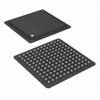
PACKAGE INFORMATION (The package drawing(s) in this data sheet may not reflect the most current specifications. The package number provided for each package is a link to the latest package outline information.) 12.1 144-Ball TE-PBGA (56-G6020-001 ...
Page 59
LQFP (56-G4011-001 ...
Page 60
... MIN TYP MAX -40 +125 +27.8 +0.1 THETA-JA (θ 27.8°C/W 23.5°C/W 21.6°C/W DESCRIPTION © 2006 Maxim Integrated Products • Printed USA DS21448 3.3V T1/E1/J1 Quad Line Interface UNITS +85 °C °C °C/W UNITS +85 °C °C °C/W °C/W ...