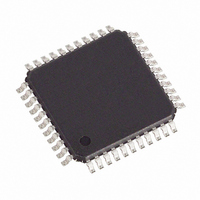
DS2148T Maxim Integrated Products, DS2148T Datasheet - Page 47

DS2148T
Manufacturer Part Number
DS2148T
Description
IC LIU E1/T1/J1 5V 44-TQFP
Manufacturer
Maxim Integrated Products
Type
Line Interface Units (LIUs)r
Specifications of DS2148T
Number Of Drivers/receivers
1/1
Protocol
T1/E1/J1
Voltage - Supply
4.75 V ~ 5.25 V
Mounting Type
Surface Mount
Package / Case
44-TQFP, 44-VQFP
Lead Free Status / RoHS Status
Contains lead / RoHS non-compliant
Available stocks
Company
Part Number
Manufacturer
Quantity
Price
Company:
Part Number:
DS2148T
Manufacturer:
TOSHIBA
Quantity:
1 057
Company:
Part Number:
DS2148T
Manufacturer:
DALLAS
Quantity:
18
Part Number:
DS2148T
Manufacturer:
DALLAS
Quantity:
20 000
Company:
Part Number:
DS2148T+
Manufacturer:
DALLAS
Quantity:
285
Company:
Part Number:
DS2148TN
Manufacturer:
DALLAS
Quantity:
12
Part Number:
DS2148TN
Manufacturer:
MAXIM/美信
Quantity:
20 000
DS2148/DS21Q48
7.2 Transmitter
The DS2148 uses a set of laser-trimmed delay lines along with a precision digital-to-analog converter
(DAC) to create the waveforms that are transmitted onto the E1 or T1 line. The waveforms created by the
DS2148 meet the latest ETSI, ITU, ANSI, and AT&T specifications. The user will select which
waveform is to be generated by setting the ETS bit (CCR1.7) for E1 or T1 operation, then programming
the L2/L1/L0 bits in Common Control Register 4 for the appropriate application. See
Table 7-1
and
Table 7-2
for the proper L2/L1/L0 settings.
A 2.048MHz or 1.544MHz TTL clock is required at TCLK for transmitting data at TPOS and TNEG.
ITU specification G.703 requires an accuracy of ±50ppm for both T1 and E1. TR62411 and ANSI specs
require an accuracy of ±32ppm for T1 interfaces. The clock can be sourced internally by RCLK or
JACLK. See CCR1.2, CCR1.1, CCR1.0, and
Figure 1-3
for details. Because of the nature of the DS2148
transmitter design, very little jitter (less than 0.005UI
broadband from 10Hz to 100kHz) is added to the
P-P
jitter present on TCLK. Also, the waveforms created are independent of the duty cycle of TCLK. The
transmitter in the DS2148 couples to the E1 or T1 transmit twisted pair (or coaxial cable in some E1
applications) via a 1:1.36 step-up transformer. In order for the device to create the proper waveforms, the
transformer used must meet the specifications listed in
Table
7-3.
The DS2148 has automatic short-circuit limiter that limits the source current to 50mA (RMS) into a 1Ω
load. This feature can be disabled by setting the SCLD bit (CCR2.5) = 1. When the current limiter is
activated, TCLE (SR.2) will be set even if short circuit limiter is disabled. The TPD bit (CCR4.0) will
power-down the transmit line driver and tri-state the TTIP and TRING pins. The DS2148 also can detect
when the TTIP or TRING outputs are open-circuited. When an open circuit is detected, TOCD (SR.1)
will be set.
7.3 Jitter Attenuator
The DS2148 contains an on-board jitter attenuator that can be set to a depth of either 32 bits or 128 bits
via the JABDS bit (CCR4.2). In hardware mode the depth is 128 bits and cannot be changed. The 128-bit
mode is used in applications where large excursions of wander are expected. The 32-bit mode is used in
delay sensitive applications. The characteristics of the attenuation are shown in
Figure
7-7. The jitter
attenuator can be placed in either the receive path or the transmit path by appropriately setting or clearing
the JAS bit (CCR4.3). Also, the jitter attenuator can be disabled (in effect, removed) by setting the DJA
bit (CCR4.1). In order for the jitter attenuator to operate properly, a 2.048MHz or 1.544MHz clock must
be applied at MCLK. ITU specification G.703 requires an accuracy of ±50ppm for both T1 and E1.
TR62411 and ANSI specs require an accuracy of ±32ppm for T1 interfaces. There is an onboard PLL for
the jitter attenuator, which will convert the 2.048MHz clock to a 1.544MHz rate for T1 applications.
Setting JAMUX (CCR1.3) to a logic 0 bypasses this PLL. On-board circuitry adjusts either the recovered
clock from the clock/data recovery block or the clock applied at the TCLK pin to create a smooth jitter-
free clock that is used to clock data out of the jitter attenuator FIFO. It is acceptable to provide a
gapped/bursty clock at the TCLK pin if the jitter attenuator is placed on the transmit side. If the incoming
jitter exceeds either 120UI
(buffer depth is 128 bits) or 28UI
(buffer depth is 32 bits), then the
P-P
P-P
DS2148 will divide the internal nominal 32.768MHz (E1) or 24.704MHz (T1) clock by either 15 or 17
instead of the normal 16 to keep the buffer from overflowing. When the device divides by either 15 or 17,
it also sets the jitter attenuator limit trip (JALT) bit in the receive information register 1 (RIR1).
47 of 73


