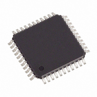
DS2148T Maxim Integrated Products, DS2148T Datasheet - Page 18

DS2148T
Manufacturer Part Number
DS2148T
Description
IC LIU E1/T1/J1 5V 44-TQFP
Manufacturer
Maxim Integrated Products
Type
Line Interface Units (LIUs)r
Specifications of DS2148T
Number Of Drivers/receivers
1/1
Protocol
T1/E1/J1
Voltage - Supply
4.75 V ~ 5.25 V
Mounting Type
Surface Mount
Package / Case
44-TQFP, 44-VQFP
Lead Free Status / RoHS Status
Contains lead / RoHS non-compliant
Available stocks
Company
Part Number
Manufacturer
Quantity
Price
Company:
Part Number:
DS2148T
Manufacturer:
TOSHIBA
Quantity:
1 057
Company:
Part Number:
DS2148T
Manufacturer:
DALLAS
Quantity:
18
Part Number:
DS2148T
Manufacturer:
DALLAS
Quantity:
20 000
Company:
Part Number:
DS2148T+
Manufacturer:
DALLAS
Quantity:
285
Company:
Part Number:
DS2148TN
Manufacturer:
DALLAS
Quantity:
12
Part Number:
DS2148TN
Manufacturer:
MAXIM/美信
Quantity:
20 000
Table 2-7. Pin Description in Hardware Mode (Sorted by Pin Name, DS2148T)
MM0/MM1
BIS0/BIS1
L0/L1/L2
JAMUX
LOOP0/
BPCLK
LOOP1
NAME
MCLK
HRST
EGL
HBE
CES
DJA
ETS
JAS
NA
32/33
16/17
18/19
7/6/5
PIN
31
12
11
29
10
30
8
1
2
9
-
I/O
O
I
I
I
I
I
I
I
I
I
I
I
I
I
I
Bus Interface Select Bits 0 & 1. Used to select bus interface option. BIS0 = 1
and BIS1 = 1 selects hardware mode.
Backplane Clock. 16.384MHz output.
Receive & Transmit Clock Edge Select. Selects which RCLK edge to update
RPOS and RNEG and which TCLK edge to sample TPOS and TNEG.
0 = update RNEG/RPOS on rising edge of RCLK; sample TPOS/TNEG on
falling edge of TCLK
1 = update RNEG/RPOS on falling edge of RCLK; sample TPOS/TNEG on
rising edge of TCLK
Disable Jitter Attenuator
0 = jitter attenuator enabled
1 = jitter attenuator disabled
Receive Equalizer Gain Limit. This pin controls the sensitivity of the receive
equalizer.
EGL E1 (ETS = 0)
0 = -12dB (short haul)
1 = -43dB (long haul)
EGL
0 = -36dB (long haul)
1 = -30dB (limited long haul)
E1/T1 Select.
0 = E1
1 = T1
Receive & Transmit HDB3/B8ZS Enable.
0 = enable HDB3 (E1)/B8ZS (T1)
1 = disable HDB3 (E1)/B8ZS (T1)
Hardware Reset. Bringing HRST low will reset the DS2148.
Jitter Attenuator MUX. Controls the source for JACLK. See
Table
MCLK = 2.048MHz
MCLK = 2.048MHz
MCLK = 1.544MHz
Jitter Attenuator Select
0 = place the jitter attenuator on the receive side
1 = place the jitter attenuator on the transmit side
Transmit LIU Waveshape Select Bits 0 & 1 [H/W Mode]. These inputs
determine the waveshape of the transmitter. See
Loopback Select Bits 0 & 1 [H/W Mode]. These inputs determine the active
loopback mode (if any). See
Master Clock. A 2.048MHz (±50ppm) clock source with TTL levels is applied
at this pin. This clock is used internally for both clock/data recovery and for jitter
attenuation. Use of a T1 1.544MHz clock source is optional. G.703 requires an
accuracy of ±50ppm for both T1 and E1. TR62411 and ANSI specs require an
accuracy of ±32ppm for T1 interfaces.
Monitor Mode Select Bits 0 & 1 [H/W Mode]. These inputs determine if the
receive equalizer is in a monitor mode. See
Not Assigned. Should be tied low.
E1 (ETS = 0)
T1 (ETS = 1)
2-13.
T1 (ETS = 1)
18 of 73
JAMUX
0
1
0
Table
FUNCTION
2-8.
Table
Table 7-1
2-11.
and
Figure 1-1
Table
7-2.
and


