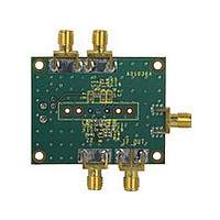
AD8342-EVAL Analog Devices Inc, AD8342-EVAL Datasheet - Page 15

AD8342-EVAL
Manufacturer Part Number
AD8342-EVAL
Description
Manufacturer
Analog Devices Inc
Datasheet
1.AD8342-EVAL.pdf
(24 pages)
Specifications of AD8342-EVAL
Lead Free Status / Rohs Status
Not Compliant
AC INTERFACES
The AD8342 is designed to downconvert radio frequencies (RF)
to lower intermediate frequencies (IF) using a high- or low-side
local oscillator (LO). The LO is injected into the mixer core at
a frequency higher or lower than the desired input RF. The
frequency difference between the LO and the RF, f
side) or f
addition to the desired RF signal, an RF image is downconverted
to the desired IF frequency. The image frequency is at f
when driven with a high-side LO. When using a broadband
load, the conversion gain of the AD8342 is nearly constant over
the specified RF input band (see Figure 3).
The AD8342 is designed to operate over a broad frequency
range. It is essential to ac couple RF and LO ports to prevent
dc offsets from skewing the mixer core in an asymmetrical
manner, potentially degrading noise figure and linearity.
The RF input of the AD8342 is high impedance, 1 kΩ across the
frequency range shown in Figure 41. The input capacitance
decreases with frequency due to package parasitics.
The matching or termination used at the RF input of the
AD8342 has a direct effect on its dynamic range. The
characterization circuit, as well as the evaluation board, uses a
100 Ω resistor to terminate the RF port. This termination
resistor in shunt with the input stage results in a return loss of
better than −10 dBm (relative to 50 Ω). Table 6 shows gain, IP3,
P1dB, and noise figure for four different input networks. This
data was measured at an RF frequency of 250 MHz and at an
LO frequency of 300 MHz.
2.00
1.75
1.50
1.25
1.00
0.75
0.50
0.25
0
0
RF
100M 200M 300M 400M 500M 600M 700M 800M 900M
− f
LO
(low side), is the intermediate frequency, f
Figure 41. RF Input Impedance
FREQUENCY (Hz)
LO
− f
1G
LO
RF
1.00
0.75
0.50
0.25
0
+ f
(high
IF
. In
IF
Rev. A | Page 15 of 24
Table 6. Dynamic Performance for Various Input Networks
Input
Network
Gain (dB)
IIP3 (dBm)
P1dB (dBm)
NF (dB)
The RF port can also be matched using an LC circuit, as shown
in Figure 42.
Impedance transformations of greater than 10:1 result in a
higher Q circuit and thus a narrow RF input bandwidth. A 1 kΩ
resistor is placed across the RF input of the device in parallel
with the device internal input impedance, creating a 500 Ω load.
This impedance is matched to as close as possible to 50 Ω for
the source, with standard components using a shunt C, series L
matching circuit (see Figure 43).
10
50Ω
POINT 1(1000 + j0) Ω
POINT 2(500 + j0) Ω
POINT 3(55.6 – j157.2) Ω
POINT 4(55.6 – j0.1) Ω
50 Ω
Shunt
0.66
25.4
10.8
14
25
100nH
Figure 43. LC Matching Example
3.6pF
Figure 42. Matching Circuit
100 Ω
Shunt
3.5
22.9
8.4
12.5
1kΩ
Q = 3
50
4
10
(1000 + j0) Ω
Z
L
25
500 Ω
Shunt
5.3
20. 6
6.3
10.2
Z
f
MAIN
50
O
= 50Ω
100
= 250MHz
100
3
200
Matched
(Figure 42)
9.3
18.5
2.3
10.5
500
2
AD8342
200
1
500


