AD8342-EVAL Analog Devices Inc, AD8342-EVAL Datasheet
AD8342-EVAL
Specifications of AD8342-EVAL


AD8342-EVAL Summary of contents
Page 1
... It is well suited for demanding receive-channel applications that require wide bandwidth on all ports and very low intermodulation distortion and noise figure. The AD8342 provides a typical conversion gain of 3.7 dB with an RF frequency of 238 MHz. The integrated LO driver presents a 50 Ω input impedance with a low LO drive level, helping to minimize the external component count ...
Page 2
... AD8342 TABLE OF CONTENTS Features .............................................................................................. 1 Applications....................................................................................... 1 Functional Block Diagram .............................................................. 1 General Description ......................................................................... 1 Revision History ............................................................................... 2 Specifications..................................................................................... 3 AC Performance ........................................................................... 4 Spur Table .......................................................................................... 5 Absolute Maximum Ratings............................................................ 6 ESD Caution.................................................................................. 6 REVISION HISTORY 1/07—Rev Rev. A Changes to Features.......................................................................... 1 Changes to General Description .................................................... 1 Changes to Table 2............................................................................ 4 Replaced the High Frequency Applications Section.................. 18 4/05— ...
Page 3
... BIAS Rev Page 1.82 kΩ, RF termination = 100 Ω, IF BIAS Min Typ Max 10 1||0.4 2.4 10||0.5 4. − 1.6 S 3.5 0.4 4 −80 +100 4. 113 500 AD8342 Unit dB kΩ||pF V kΩ||pF V dBm μs μs μA μ μA ...
Page 4
... AD8342 AC PERFORMANCE 25°C, LO power = 0 dBm unless otherwise noted. Table 2. Parameter Conditions 1 RF Frequency Range 1 LO Frequency Range 1 IF Frequency Range Conversion Gain SSB Noise Figure Input Third-Order Intercept f RF1 f IF1 f RF1 f IF1 Input Second-Order Intercept f RF1 f IF2 f RF1 f IF2 Input 1 dB Compression Point ...
Page 5
... AD8342 13 14 −46 −59 −37 −61 −67 −79 −90 −81 <−100 −95 <−100 <−100 <−100 <−100 <−100 <−100 <−100 <−100 < ...
Page 6
... AD8342 ABSOLUTE MAXIMUM RATINGS Table 4. Parameter Supply Voltage Input Level LO Input Level PWDN Pin IFOP, IFOM Bias Voltage Minimum Resistor from EXRB to COMM Internal Power Dissipation θ JA Maximum Junction Temperature Operating Temperature Range Storage Temperature Range Stresses above those listed under Absolute Maximum Ratings may cause permanent damage to the device ...
Page 7
... Positive Supply Voltage for the Mixer: 4. 5.25 V. PIN 1 12 VPDC VPLO 1 INDICATOR LOCM 2 11 PWDN AD8342 LOIN 3 10 EXRB TOP VIEW COMM 4 (Not to Scale) 9 COMM Figure 2. 16-Lead LFCSP − 1.6 V. Must be ac-coupled. S Rev Page AD8342 − 1.6 V. AC-couple to ground. S for disable mode. S ...
Page 8
... AD8342 TYPICAL PERFORMANCE CHARACTERISTICS 25°C, RF power = −10 dBm, LO power = 0 dBm 100 Ω via a 2:1 ratio balun, unless otherwise noted 48MHz 140MHz IF = 10MHz IF = 90MHz 100 150 200 250 300 350 RF FREQUENCY (MHz) Figure 3. Conversion Gain vs. RF Frequency 48MHz 140MHz IF = 90MHz –15 –10 – ...
Page 9
... VPOS (V) = 238 MHz 239 MHz RF RF2 LO Frequency = 286 MHz NORMAL MEAN = 22.7 STD. DEV. = 0.41 21.0 21.4 21.8 22.2 22.6 23.0 23.4 INPUT IP3 (238MHz) = 238 MHz AD8342 300 350 5.20 5.25 23.8 24.2 = 286 MHz ...
Page 10
... AD8342 90MHz 48MHz 7 140MHz 100 150 200 250 300 350 RF FREQUENCY (MHz) Figure 15. Input P1dB vs. RF Frequency 10.0 9 10MHz 9 90MHz 8.5 8 140MHz 7 48MHz 7.0 6.5 6.0 5.5 5.0 –15 –13 –11 –9 –7 –5 –3 LO LEVEL (dBm) Figure 16. Input P1dB vs. LO Level, f ...
Page 11
... IF FREQUENCY (MHz) 4.85 4.95 5.05 5.15 VPOS (V) Figure 25. Input IP2 vs. VPOS 238 MHz, RF1 f = 188 MHz 286 MHz RF2 460MHz RF = 238MHz 60 110 160 210 260 IF FREQUENCY (MHz) Figure 26. Noise Figure vs. IF Frequency AD8342 350 5.25 310 ...
Page 12
... AD8342 140MHz NF = 90MHz 10MHz 11 10 –15 –13 –11 –9 –7 –5 –3 LO POWER (dBm) Figure 27. Noise Figure vs. LO Power, f 5.0 4.5 4.0 3.5 3.0 2.5 2.0 1.5 1.0 0.5 0 1.8 2.0 2.2 2.4 2.6 2.8 R (kΩ) BIAS Figure 28. Gain vs Frequency = 238 MHz, LO Frequency = 286 MHz ...
Page 13
... VPDC PWDN EXRB COMM 13 COMM 8 COMM 1nF 7 14 RFCM IFOP AD8342 100Ω 15 RFIN 6 IFOM 1nF 5 16 VPMX COMM 100pF VPLO LOCM LOIN COMM 100pF 1nF 1nF 100pF LO IN Characteristics Data AD8342 80 860 IF OUT (50Ω) TC2-1T VPOS 0.1µF ...
Page 14
... The device also features a power-down function. Application of a logic low at the PWDN pin allows normal operation. A high logic level at the PWDN pin shuts down the AD8342. Power consumption when the part is disabled is less than 10 mW. The bias for the mixer is set with an external resistor (R from the EXRB pin to ground ...
Page 15
... It is essential to ac couple RF and LO ports to prevent dc offsets from skewing the mixer core in an asymmetrical manner, potentially degrading noise figure and linearity. The RF input of the AD8342 is high impedance, 1 kΩ across the frequency range shown in Figure 41. The input capacitance decreases with frequency due to package parasitics. ...
Page 16
... PCB traces. One approach is to use an impedance transforming network or transformer located close to the AD8342. If very wideband output is desired, a nearby buffer amplifier may be a better choice, especially if IF response required. An example of such a circuit is presented in Figure 45, in which the differential amplifier is used to drive a pair of 75 Ω ...
Page 17
... COMM 5 Figure 48. Biasing the IF Port Open-Collector Outputs Using Pull-Up Choke Inductors The AD8342 is optimized for driving a 100 Ω load. Although the device is capable of driving a wide variety of loads, to maintain optimum distortion and noise performance advised that the presented load at the IF outputs is close to 100 Ω ...
Page 18
... MHz band possible to use purely reactive matching to transform a 50 Ω source to match the raw ~1 kΩ input impedance of the AD8342. However, the L and C component variations could present production concerns due to the sensitivity of the match. For this application advantageous to shunt down the ~1 kΩ ...
Page 19
... RF FREQUENCY (MHz) Figure 54. Input OIP3, IP1dB, Gain and NF vs. RF Frequency for a 190 MHz IF Using a Low-Side LO. The broadband frequency capabilities of the AD8342 makes it an attractive solution for a variety of applications, including cellular, CATV, point-to-point radio links, and test equipment example, the circuit depicted in Figure 53 can easily be applied as a feedback mixer in a predistortion receiver design ...
Page 20
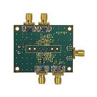
... AD8342 EVALUATION BOARD An evaluation board is available for the AD8342. The evaluation board is configured for single-ended signaling at the IF output port via a balun transformer. The schematic for the evaluation board is presented in Figure 56. PWDN PWDN W1 GND VPOS R7 VPOS 0Ω C12 0.1µF L1 1000pF 50Ω ...
Page 21
... SEATING PLANE ORDERING GUIDE Model Temperature Range 1 AD8342ACPZ-REEL7 −40°C to +85°C 1 AD8342ACPZ-R2 −40°C to +85°C 1 AD8342ACPZ-WP −40°C to +85°C 1 AD8342-EVALZ Pb-free part. 3.00 0.60 MAX BSC SQ 0. 2.75 TOP BSC SQ VIEW 9 (BOTTOM VIEW) 0.50 8 BSC 1 ...
Page 22
... AD8342 NOTES Rev Page ...
Page 23
... NOTES Rev Page AD8342 ...
Page 24
... AD8342 NOTES ©2007 Analog Devices, Inc. All rights reserved. Trademarks and registered trademarks are the property of their respective owners. D05352-0-1/07(A) Rev Page ...