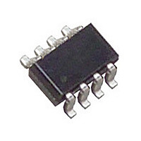
LTC2934ITS8-1#PBF Linear Technology, LTC2934ITS8-1#PBF Datasheet - Page 5

LTC2934ITS8-1#PBF
Manufacturer Part Number
LTC2934ITS8-1#PBF
Description
Manufacturer
Linear Technology
Datasheet
1.LTC2934ITS8-1PBF.pdf
(12 pages)
Specifications of LTC2934ITS8-1#PBF
Lead Free Status / Rohs Status
Compliant
Available stocks
Company
Part Number
Manufacturer
Quantity
Price
PIN FUNCTIONS
TYPICAL PERFORMANCE CHARACTERISTICS
ADJ: Reset Threshold Adjustment Input. Tie to resistive
divider between monitored voltage and GND to confi gure
desired reset threshold. See the Applications Information
section for details. Tie to V
Exposed Pad (DFN Only): Exposed Pad may be left fl oating
or connected to device ground.
GND: Device Ground.
MR: Manual Reset Input. Attach a push-button switch
between this input and ground. A logic low on this input
pulls RST low. When the MR input returns to logic high,
RST returns high after the reset timer has expired. Tie to
V
PFI: Power-Fail Threshold Adjustment Input. Tie to
resistive divider between monitored voltage and GND
to configure desired power-fail threshold. See the
Applications Information section for details. Tie to V
GND if unused.
CC
if unused.
250
200
150
100
50
0
0
Supply Current vs RT
Input Voltage
V
CC
0.5
= 3.6V
CC
1
RT INPUT VOLTAGE (V)
if unused.
1.5
2
2.5
3
3.5
2934 G07
4
CC
or
PFO: Power-Fail Output. PFO pulls low when monitored
voltage falls below the power-fail (PFI) threshold. PFO
is released when the PFI voltage rises above the power-
fail threshold by 2.5%. PFO is available with open-drain
(LTC2934-1) or active pull-up (LTC2934-2) outputs. Leave
open if unused.
RST: Reset Output. RST pulls low when monitored volt-
age falls below the reset threshold. RST is released after
monitored voltage exceeds the reset threshold plus 5%
hysteresis and after reset timer has expired. RST is available
with open-drain (LTC2934-1) or active pull-up (LTC2934-2)
outputs. Leave open if unused.
RT: Reset Timeout Selection Input. Tie to GND or V
desired reset timeout. Tie low for 15ms delay or high for
200ms delay.
V
GND.
CC
: Power Supply Input. Bypass V
5
4
3
2
0
1
0
Supply Current vs MR Input Voltage
0.5
T
A
1
MR INPUT VOLTAGE (V)
= 25°C, unless otherwise noted.
1.5
2
2.5
3
V
CC
= 3.6V
3.5
2934 G08
4
CC
LTC2934
with 0.1μF to
CC
5
2934f
for


