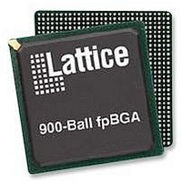
LFE2M70E-5FN900C Lattice, LFE2M70E-5FN900C Datasheet - Page 104

LFE2M70E-5FN900C
Manufacturer Part Number
LFE2M70E-5FN900C
Description
IC, LATTICEECP2M FPGA, 420MHZ, FPBGA-900
Manufacturer
Lattice
Series
LatticeECP2Mr
Datasheet
1.LFE2-12E-5FN256C.pdf
(385 pages)
Specifications of LFE2M70E-5FN900C
No. Of Logic Blocks
67000
No. Of Macrocells
34000
No. Of Speed Grades
5
Total Ram Bits
4534Kbit
No. Of I/o's
416
Clock Management
DLL, PLL
I/o Supply Voltage
3.465V
Rohs Compliant
Yes
Lead Free Status / Rohs Status
Lead free / RoHS Compliant
Available stocks
Company
Part Number
Manufacturer
Quantity
Price
Company:
Part Number:
LFE2M70E-5FN900C
Manufacturer:
Lattice Semiconductor Corporation
Quantity:
10 000
- Current page: 104 of 385
- Download datasheet (3Mb)
Lattice Semiconductor
PICs and DDR Data (DQ) Pins Associated with the DDR Strobe (DQS) Pin
For Left and Right Edges of the Device
P[Edge] [n-4]
P[Edge] [n-3]
P[Edge] [n-2]
P[Edge] [n-1]
P[Edge] [n]
P[Edge] [n+1]
P[Edge] [n+2]
P[Edge] [n+3]
For Bottom Edge of the Device
P[Edge] [n-4]
P[Edge] [n-3]
P[Edge] [n-2]
P[Edge] [n-1]
P[Edge] [n]
P[Edge] [n+1]
P[Edge] [n+2]
P[Edge] [n+3]
P[Edge] [n+4]
Notes:
1. “n” is a row PIC number.
2. The DDR interface is designed for memories that support one DQS strobe up to 15 bits
PICs Associated with
of data for the left and right edges and up to 17 bits of data for the bottom edge. In some
packages, all the potential DDR data (DQ) pins may not be available. PIC numbering
definitions are provided in the “Signal Names” column of the Signal Descriptions table.
DQS Strobe
PIO Within PIC
4-4
A
B
A
B
A
B
A
B
A
B
A
B
A
B
A
B
A
B
A
B
A
B
A
B
A
B
A
B
A
B
A
B
A
B
DDR Strobe (DQS) and
LatticeECP2/M Family Data Sheet
Data (DQ) Pins
[Edge]DQSn
[Edge]DQSn
DQ
DQ
DQ
DQ
DQ
DQ
DQ
DQ
DQ
DQ
DQ
DQ
DQ
DQ
DQ
DQ
DQ
DQ
DQ
DQ
DQ
DQ
DQ
DQ
DQ
DQ
DQ
DQ
DQ
DQ
DQ
DQ
Pinout Information
Related parts for LFE2M70E-5FN900C
Image
Part Number
Description
Manufacturer
Datasheet
Request
R
Part Number:
Description:
Manufacturer:
Lattice Semiconductor Corp.
Datasheet:
Part Number:
Description:
IC, LATTICEECP2M FPGA, 420MHZ, FPBGA-900
Manufacturer:
LATTICE SEMICONDUCTOR
Datasheet:

Part Number:
Description:
IC FPGA 50KLUTS 410I/O 900-BGA
Manufacturer:
Lattice
Datasheet:

Part Number:
Description:
IC FPGA 50KLUTS 410I/O 900-BGA
Manufacturer:
Lattice
Datasheet:

Part Number:
Description:
IC FPGA 67KLUTS 1152FPBGA
Manufacturer:
Lattice
Datasheet:

Part Number:
Description:
IC FPGA 67KLUTS 900FPBGA
Manufacturer:
Lattice
Datasheet:

Part Number:
Description:
IC FPGA 67KLUTS 1152FPBGA
Manufacturer:
Lattice
Datasheet:

Part Number:
Description:
IC FPGA 67KLUTS 1152FPBGA
Manufacturer:
Lattice
Datasheet:

Part Number:
Description:
IC FPGA 67KLUTS 1152FPBGA
Manufacturer:
Lattice
Datasheet:

Part Number:
Description:
FPGA - Field Programmable Gate Array 67K LUTs 430 I/O Memry DSP 1.2V -5Spd
Manufacturer:
Lattice

Part Number:
Description:
FPGA - Field Programmable Gate Array 67K LUTs 430 I/O Memry DSP 1.2V -7Spd
Manufacturer:
Lattice

Part Number:
Description:
FPGA - Field Programmable Gate Array 67K LUTs 430 I/O Memry DSP 1.2V -5Spd
Manufacturer:
Lattice

Part Number:
Description:
FPGA - Field Programmable Gate Array 67K LUTs 430 I/O Memry DSP 1.2V -6Spd
Manufacturer:
Lattice

Part Number:
Description:
FPGA - Field Programmable Gate Array 67K LUTs 416 I/O Memory DSP 1.2V 5SPD
Manufacturer:
Lattice


