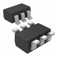
MAX9130EXT+T Maxim Integrated Products, MAX9130EXT+T Datasheet - Page 6

MAX9130EXT+T
Manufacturer Part Number
MAX9130EXT+T
Description
IC RCVR SNGL LVDS SC70-6
Manufacturer
Maxim Integrated Products
Type
Receiverr
Datasheet
1.MAX9130EXTT.pdf
(8 pages)
Specifications of MAX9130EXT+T
Number Of Drivers/receivers
0/1
Protocol
LVDS
Voltage - Supply
3 V ~ 3.6 V
Mounting Type
Surface Mount
Package / Case
SC-70-6, SC-88, SOT-363
Lead Free Status / RoHS Status
Lead free / RoHS Compliant
LVDS is intended for point-to-point communication over
a controlled-impedance medium as defined by the
ANSI TIA/EIA-644 and IEEE 1596.3 standards. LVDS
uses a lower voltage swing than other common com-
munication standards, achieving higher data rates with
reduced power consumption while reducing EMI emis-
sions and system susceptibility to noise.
The MAX9130 is a single LVDS line receiver ideal for
applications requiring high data rates, low power, and
low noise. The device accepts an LVDS input and
translates it to an LVTTL/LVCMOS output. The receiver
detects differential signals as low as 50mV and as high
as 1V within an input voltage range of 0 to +2.4V.
The 250mV to 450mV differential output of an LVDS dri-
ver is nominally centered around a +1.25V offset. This
offset, coupled with the receiver’s 0 to +2.4V input volt-
age range, allows an approximate ±1V shift in the sig-
nal (as seen by the receiver). This allows for a
difference in ground references of the driver and the
receiver, the common-mode effects of coupled noise,
or both. The LVDS standards specify an input voltage
range of 0 to +2.4V referenced to receiver ground.
The fail-safe feature of the MAX9130 sets the output
high and reduces supply current to 150µA when:
• inputs are open
• inputs are undriven and shorted
• inputs are undriven and terminated
A fail-safe circuit is important because under these
conditions, noise at the input may switch the receiver
and it may appear to the system that data is being
received. Open or undriven terminated input conditions
can occur when a cable is disconnected or cut, or
when an LVDS driver output is in high impedance. A
short condition can occur because of a cable failure.
Single 500Mbps LVDS Line Receiver in SC70
6
PIN
2, 5
_______________________________________________________________________________________
1
3
4
6
NAME
GND
OUT
V
IN+
IN-
CC
Power-Supply Input. Bypass V
GND with a 0.01µF ceramic capacitor.
Ground
Inverting LVDS Differential Input
Noninverting LVDS Differential Input
LVTTL/LVCMOS Output
Detailed Description
Pin Description
FUNCTION
Fail-Safe
CC
to
The fail-safe input network (Figure 1) samples the input
common-mode voltage and compares it to V
(nominal). When the input is driven to levels specified in
the LVDS standards, the input common-mode voltage
is less than V
activated. If the inputs are open or if the inputs are
undriven and shorted or undriven and parallel terminat-
ed, there is no input current. In this case, a pullup resis-
tor in the fail-safe circuit pulls both inputs above V
0.3V, activating the fail-safe circuit and forcing the out-
put high.
Bypass V
ceramic 0.01µF capacitor as close to the device as
possible.
Figure 1. Fail-Safe Input Network
Figure 2. Propagation Delay and Transition Time Test Circuit
IN+
IN-
*50Ω REQUIRED FOR PULSE GENERATOR.
GENERATOR
CC
PULSE
R
R
IN1
IN1
*50Ω
CC
with a high-frequency surface-mount
Applications Information
R
IN2
- 0.3V and the fail-safe circuit is not
V
CC
Power-Supply Bypassing
V
CC
*50Ω
GND
- 0.3V
IN+
IN-
MAX9130
Rx
MAX9130
C
L
OUT
CC
OUT
- 0.3V
CC
-


