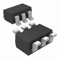
MAX9130EXT+T Maxim Integrated Products, MAX9130EXT+T Datasheet - Page 2

MAX9130EXT+T
Manufacturer Part Number
MAX9130EXT+T
Description
IC RCVR SNGL LVDS SC70-6
Manufacturer
Maxim Integrated Products
Type
Receiverr
Datasheet
1.MAX9130EXTT.pdf
(8 pages)
Specifications of MAX9130EXT+T
Number Of Drivers/receivers
0/1
Protocol
LVDS
Voltage - Supply
3 V ~ 3.6 V
Mounting Type
Surface Mount
Package / Case
SC-70-6, SC-88, SOT-363
Lead Free Status / RoHS Status
Lead free / RoHS Compliant
ABSOLUTE MAXIMUM RATINGS
V
IN+, IN- to GND.....................................................-0.3V to +4.0V
OUT to GND ...............................................-0.3V to (V
Continuous Power Dissipation (T
Output Short to GND (OUT) (Note 1)........................................1s
Storage Temperature Range .............................-65°C to +150°C
Single 500Mbps LVDS Line Receiver in SC70
Note 1: Package leads soldered to a PC board having copper ground and V
Stresses beyond those listed under “Absolute Maximum Ratings” may cause permanent damage to the device. These are stress ratings only, and functional
operation of the device at these or any other conditions beyond those indicated in the operational sections of the specifications is not implied. Exposure to
absolute maximum rating conditions for extended periods may affect device reliability.
DC ELECTRICAL CHARACTERISTICS
(V
T
2
LVDS INPUTS (IN+, IN-)
Differential Input High Threshold
Differential Input Low Threshold
Input Current
Power-Off Input Current
Input Resistance
LVTTL/LVCMOS OUTPUT (OUT)
Output High Voltage
Output Low Voltage
Output Short-Circuit Current
SUPPLY CURRENT
Supply Current
CC
A
CC
6-Pin SC70 (derate 3.1mW/°C above +70°C) .............245 mW
= -40°C to +85°C, unless otherwise noted. Typical values at V
_______________________________________________________________________________________
to GND ...........................................................-0.3V to +4.0V
= +3.0V to +3.6V, differential input voltage |V
PARAMETER
A
= +70°C)
SYMBOL
I
IN+
V
I
V
V
V
R
R
I
I
INO
OS
CC
OL
TH
OH
TL
, I
IN1
IN2
IN-
0.05V ≤V
0.6V <V
0.05V ≤V
0.6V <V
V
V
I
I
V
No load, inputs undriven (fail-safe)
No load, inputs driven
OH
OL
CC
CC
ID
= - 8.0m A
= +8.0mA, V
= +50mV, V
CC
= +3.6V or 0, Figure 1
= +3.6V or 0, Figure 1
ID
+ 0.3V)
| = 0.05V to 1.0V, input common voltage V
ID
ID
ID
ID
≤ 1.0V
≤ 1.0V, V
≤ 0.6V
≤ 0.6V, V
CONDITIONS
OUT
CC
Inp uts op en or und r i ven shor t
or und r i ven 100Ω ter m i nati on
V
ID
ID
= -50mV
= +3.3V, T
= +50mV
= 0
Maximum Junction Temperature .....................................+150°C
Operating Temperature Range ...........................-40°C to +85°C
ESD Protection
Lead Temperature (soldering, 10s) .................................+300°C
CC
CC
Human Body Model (IN+, IN-) .........................................±6kV
= 0
= 0
CC
planes. Do not exceed Maximum Junction Temperature.
A
= +25°C.) (Notes 2, 3)
V
V
MIN
132
CC
CC
-50
-20
-25
-20
-25
35
- 0.3
- 0.3
CM
= |V
TYP
150
ID
/2| to 2.4V - |V
MAX
0.25
-125
300
50
20
25
20
25
7
UNITS
mA
mA
mV
mV
µA
µA
kΩ
µA
V
V
ID
/2|,


