CLC014AJE National Semiconductor, CLC014AJE Datasheet - Page 15
CLC014AJE
Manufacturer Part Number
CLC014AJE
Description
07B4822
Manufacturer
National Semiconductor
Specifications of CLC014AJE
Ic Function
Adaptive Cable Equalizer
Supply Voltage Range
4.5V To 5.5V
Operating Temperature Range
-40°C To +85°C
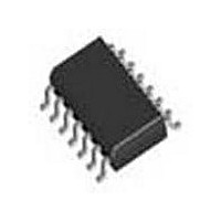
Digital Ic Case Style
SOIC
No. Of Pins
14
Termination Type
SMD
Rohs Compliant
No
Filter Terminals
SMD
Data Rate Max
650Mbps
Lead Free Status / Rohs Status
Not Compliant
Available stocks
Company
Part Number
Manufacturer
Quantity
Price

Company:
Part Number:
CLC014AJE
Manufacturer:
NS
Quantity:
5 000
Part Number:
CLC014AJE
Manufacturer:
NS/国半
Quantity:
20 000
Company:
Part Number:
CLC014AJE-TR13
Manufacturer:
NS
Quantity:
20
Company:
Part Number:
CLC014AJE/NOPB
Manufacturer:
NSC
Quantity:
772


Evaluation Board
Evaluation boards are available for a nominal charge that
demonstrate the basic operation of the SDI/SDV/SDH de-
vices. The evaluation boards can be ordered through
National's Distributors. Supplies are limited, please check for
current availability.
The SD014EVK evaluation kit for the CLC014, Adaptive Ca-
ble Equalizer for High-Speed Data Recovery, provides an
operating environment in which the cable equalizer can be
evaluated by system / hardware designers. The evaluation
board has all the needed circuitry and connectors for easy
connection and checkout of the device circuit options as dis-
cussed in the CLC014 datasheet. A schematic, parts list and
pictorial drawing are provided with the board.
From the WWW, the following information may be viewed /
downloaded for most evaluation boards: www.national.com/
appinfo/interface
•
Device Datasheet and / or EVK User Manual
100056 Version 11 Revision 6
15
Print Date/Time: 2010/08/23 16:48:25
•
•
•
•
PCB LAYOUT
The CLC014 requires proper high-speed layout techniques to
obtain best results. A few recommended layout rules to follow
for best results when using the CLC014 Adaptive Cable
Equalizer are:
1.
2.
3.
4.
5.
View a picture of the EVK
View the EVK Schematic
View the top assembly drawing and BOM
View the bottom assembly drawing and BOM
Use a ground plane.
Decouple power pins with 0.01 μF capacitors placed
≤
Design transmission lines to the inputs and outputs.
Route outputs away from inputs.
Remove ground plane
and output pads.
0.1” (3mm) from the power pins.
≥
0.025” (0.06mm) from the input
www.national.com
Related parts for CLC014AJE
Image
Part Number
Description
Manufacturer
Datasheet
Request
R

Part Number:
Description:
Adaptive Cable Equalizer for High-Speed Data Recovery
Manufacturer:
National Semiconductor
Part Number:
Description:
National Semiconductor [8-Bit D/A Converter]
Manufacturer:
National Semiconductor
Datasheet:
Part Number:
Description:
National Semiconductor [Media Coprocessor]
Manufacturer:
National Semiconductor
Datasheet:
Part Number:
Description:
Digitally Controlled Tone and Volume Circuit with Stereo Audio Power Amplifier, Microphone Preamp Stage and National 3D Sound
Manufacturer:
National Semiconductor
Datasheet:
Part Number:
Description:
Digitally Controlled Tone and Volume Circuit with Stereo Audio Power Amplifier, Microphone Preamp Stage and National 3D Sound
Manufacturer:
National Semiconductor
Datasheet:
Part Number:
Description:
AC97 Rev 2 Codec with Sample Rate Conversion and National 3D Sound
Manufacturer:
National Semiconductor
Part Number:
Description:
Manufacturer:
National Semiconductor
Datasheet:
Part Number:
Description:
Manufacturer:
National Semiconductor
Datasheet:
Part Number:
Description:
General Purpose, Low Voltage, Low Power, Rail-to-Rail Output Operational Amplifiers
Manufacturer:
National Semiconductor
Datasheet:
Part Number:
Description:
8-bit 20 MSPS flash A/D converter.
Manufacturer:
National Semiconductor
Datasheet:
Part Number:
Description:
Low Noise Quad Operational Amplifier
Manufacturer:
National Semiconductor
Datasheet:
Part Number:
Description:
Quad Differential Line Receivers
Manufacturer:
National Semiconductor
Datasheet:
Part Number:
Description:
Quad High Speed Trapezoidal? Bus Transceiver
Manufacturer:
National Semiconductor
Datasheet:
Part Number:
Description:
Dual Line Receiver
Manufacturer:
National Semiconductor
Datasheet: