CLC014AJE National Semiconductor, CLC014AJE Datasheet - Page 11
CLC014AJE
Manufacturer Part Number
CLC014AJE
Description
07B4822
Manufacturer
National Semiconductor
Specifications of CLC014AJE
Ic Function
Adaptive Cable Equalizer
Supply Voltage Range
4.5V To 5.5V
Operating Temperature Range
-40°C To +85°C
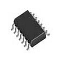
Digital Ic Case Style
SOIC
No. Of Pins
14
Termination Type
SMD
Rohs Compliant
No
Filter Terminals
SMD
Data Rate Max
650Mbps
Lead Free Status / Rohs Status
Not Compliant
Available stocks
Company
Part Number
Manufacturer
Quantity
Price

Company:
Part Number:
CLC014AJE
Manufacturer:
NS
Quantity:
5 000
Part Number:
CLC014AJE
Manufacturer:
NS/国半
Quantity:
20 000
Company:
Part Number:
CLC014AJE-TR13
Manufacturer:
NS
Quantity:
20
Company:
Part Number:
CLC014AJE/NOPB
Manufacturer:
NSC
Quantity:
772


Layout and Measurement
The printed circuit board layout for the CLC014 requires prop-
er high-speed layout to achieve the performance specifica-
tions found in the datasheet. The following list contains a few
rules to follow:
1.
2.
3.
4.
5.
Troubleshooting with scope probes can affect the equaliza-
tion. For high data rates, use a low capacitance probe with
less than 2 pF probe capacitance. Evaluation boards and lit-
erature are available for quick prototyping and evaluation of
the CLC014 Adaptive Cable Equalizer. The CLC014 contains
CMOS devices and operators should use grounding straps
when handling the parts.
Figure 9
Bypass V
•
•
Monolithic capacitor of about 0.1 μF placed less than
0.1” (3mm) from the pin
Tantalum capacitor of about 6.8 μF for large current signal
swings placed as close as convenient to the CLC014
Use a ground plane.
Decouple power pins with 0.1 μF capacitors placed
≤
Design transmission strip lines from the CLC014's input
and output pins to the board connectors.
Route outputs away from inputs.
Keep ground plane
input and output pads.
0.1” (3mm) from the power pins.
shows the CLC014's internal power supply routing.
CC
(pin 4) by:
≥
0.025” (0.06mm) away from the
100056 Version 11 Revision 6
FIGURE 8. Typical Measurement Block
11
Print Date/Time: 2010/08/23 16:48:25
Figure 8
Figure 15
pattern generator with low output jitter was used to provide a
NRZI pattern to create the eye diagrams shown in the Typical
Performance Characteristics section.
Since most pattern generators have a 50Ω output impedance,
a translation can be accomplished using a CLC006 Cable
Driver as an impedance transformer. A wide bandwidth os-
cilloscope is needed to observe the high data rate eye pattern.
When monitoring a single output that is terminated at both the
equalizer output and the oscilloscope, the effective output
load is 37.5Ω. Consequently, the signal swing is half that ob-
served for a single-ended 75Ω termination.
FIGURE 9. Power Package Routing Fixture
shows a block level measurement diagram, while
on depicts a detailed schematic. A pseudo-random
www.national.com
10005629
10005628
Related parts for CLC014AJE
Image
Part Number
Description
Manufacturer
Datasheet
Request
R

Part Number:
Description:
Adaptive Cable Equalizer for High-Speed Data Recovery
Manufacturer:
National Semiconductor
Part Number:
Description:
National Semiconductor [8-Bit D/A Converter]
Manufacturer:
National Semiconductor
Datasheet:
Part Number:
Description:
National Semiconductor [Media Coprocessor]
Manufacturer:
National Semiconductor
Datasheet:
Part Number:
Description:
Digitally Controlled Tone and Volume Circuit with Stereo Audio Power Amplifier, Microphone Preamp Stage and National 3D Sound
Manufacturer:
National Semiconductor
Datasheet:
Part Number:
Description:
Digitally Controlled Tone and Volume Circuit with Stereo Audio Power Amplifier, Microphone Preamp Stage and National 3D Sound
Manufacturer:
National Semiconductor
Datasheet:
Part Number:
Description:
AC97 Rev 2 Codec with Sample Rate Conversion and National 3D Sound
Manufacturer:
National Semiconductor
Part Number:
Description:
Manufacturer:
National Semiconductor
Datasheet:
Part Number:
Description:
Manufacturer:
National Semiconductor
Datasheet:
Part Number:
Description:
General Purpose, Low Voltage, Low Power, Rail-to-Rail Output Operational Amplifiers
Manufacturer:
National Semiconductor
Datasheet:
Part Number:
Description:
8-bit 20 MSPS flash A/D converter.
Manufacturer:
National Semiconductor
Datasheet:
Part Number:
Description:
Low Noise Quad Operational Amplifier
Manufacturer:
National Semiconductor
Datasheet:
Part Number:
Description:
Quad Differential Line Receivers
Manufacturer:
National Semiconductor
Datasheet:
Part Number:
Description:
Quad High Speed Trapezoidal? Bus Transceiver
Manufacturer:
National Semiconductor
Datasheet:
Part Number:
Description:
Dual Line Receiver
Manufacturer:
National Semiconductor
Datasheet: