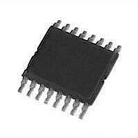
STLVDS3487BD STMicroelectronics, STLVDS3487BD Datasheet

STLVDS3487BD
Specifications of STLVDS3487BD
Available stocks
Related parts for STLVDS3487BD
STLVDS3487BD Summary of contents
Page 1
Feature summary Meets or exceeds the requirements of ansi TIA/EIA-644 standard Low voltage differential signaling with typical output voltage of 350mV and a 100 Typical output voltage rise and fall times of 750ps (400Mbps) Typical propagation delay times of 1.7ns ...
Page 2
Contents 1 Pin configuration . . . . . . . . . . . . . . . . . . . . . . . . . . . . . . . . . . . . ...
Page 3
STLVDS3487 1 Pin configuration Figure 1. Pin connections Table 1. Pin description Pin n° 10 11 Table 2. Truth table Input OPEN ...
Page 4
Logic diagram 2 Logic diagram Figure 2. Logic diagram and logic symbol 4/16 STLVDS3487 ...
Page 5
STLVDS3487 3 Maximum ratings Table 3. Absolute maximum ratings Symbol V Supply voltage (Note Input voltage I T Storage temperature range stg Note: Absolute Maximum Ratings are those values beyond which damage to the device may ...
Page 6
Electrical characteristics 4 Electrical characteristics Table 5. Electrical characteristics (Over recommended operating conditions unless otherwise noted. All typical values are 25°C, and Symbol Parameter V Differential output voltage OD Change in differential output V ...
Page 7
STLVDS3487 Table 6. Switching characteristics (Over recommended operating conditions unless otherwise noted. All typical values are 25°C, and Symbol Parameter Propagation Delay Time, Low to t PLH High Output Propagation Delay Time, High to ...
Page 8
Test circuit 5 Test circuit Figure 3. Voltage and current definitions Figure 4. Test circuit, timing and voltage definitions for differential output signal Note A: All input pulse are supplied by a generator having the following characteristics ...
Page 9
STLVDS3487 Figure 5. Test circuit and definitions for the driver common mode output voltage Note A: All input pulse are supplied by a generator having the following characteristics 1ns, pulse repetition rate (PRR) = 50Mpps, pulse width ...
Page 10
Test circuit Figure 6. Enable and disable time test circuit and waveform Note A: All input pulse are supplied by a generator having the following characteristics 1ns, pulse repetition rate (PRR) = 0.5Mpps, pulse width = 500 ...
Page 11
STLVDS3487 6 Typical performance characteristics (unless otherwise specified at T Figure 7. Supply current vs temperature Figure 9. Propagation delay enable to output Figure 10. Propagation delay time Figure 11. Differential output signal Typical performance characteristics = 25°C) J Figure ...
Page 12
Package mechanical data 7 Package mechanical data In order to meet environmental requirements, ST offers these devices in ECOPACK packages. These packages have a Lead-free second level interconnect. The category of second Level Interconnect is marked on the package and ...
Page 13
STLVDS3487 DIM. MIN 0.05 A2 0.8 b 0.19 c 0.09 D 4.9 E 6 0° PIN 1 IDENTIFICATION 1 TSSOP16 MECHANICAL DATA mm. TYP MAX. 1.2 0.15 1 ...
Page 14
Package mechanical data Tape & Reel TSSOP16 MECHANICAL DATA DIM. MIN 12 6.7 Bo 5.3 Ko 1.6 Po 3.9 P 7.9 14/16 mm. TYP MAX. MIN. 330 13.2 0.504 0.795 2.362 22.4 ...
Page 15
STLVDS3487 8 Revision history Table 7. Revision history Date Revision 06-Apr-2006 2 Order codes has been updated and new template. Revision history Changes 15/16 ...
Page 16
... Information in this document is provided solely in connection with ST products. STMicroelectronics NV and its subsidiaries (“ST”) reserve the right to make changes, corrections, modifications or improvements, to this document, and the products and services described herein at any time, without notice. All ST products are sold pursuant to ST’s terms and conditions of sale. ...


