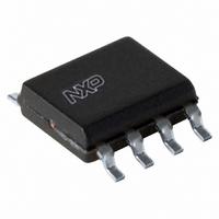
TJA1051T,118 NXP Semiconductors, TJA1051T,118 Datasheet - Page 6

TJA1051T,118
Manufacturer Part Number
TJA1051T,118
Description
IC CAN TXRX HI-SPEED 8-SOIC
Manufacturer
NXP Semiconductors
Type
Transceiverr
Datasheet
1.TJA1051T118.pdf
(21 pages)
Specifications of TJA1051T,118
Package / Case
8-SOIC (3.9mm Width)
Number Of Drivers/receivers
1/1
Protocol
CAN
Voltage - Supply
4.5 V ~ 5.5 V
Mounting Type
Surface Mount
Product
Controller Area Network (CAN)
Number Of Transceivers
1
Data Rate
1 Mbps
Supply Voltage (max)
5.5 V
Supply Voltage (min)
2.8 V or 4.5 V
Supply Current (max)
0.5 mA or 70 mA
Maximum Operating Temperature
+ 125 C
Minimum Operating Temperature
- 40 C
Mounting Style
SMD/SMT
Lead Free Status / RoHS Status
Lead free / RoHS Compliant
Lead Free Status / RoHS Status
Lead free / RoHS Compliant, Lead free / RoHS Compliant
Other names
935285281118
NXP Semiconductors
TJA1051
Product data sheet
7.1.3 Off mode
7.2.1 TXD dominant time-out function
7.2.2 Internal biasing of TXD, S and EN input pins
7.2.3 Undervoltage detection on pins V
7.2.4 Overtemperature protection
7.2 Fail-safe features
7.3 V
A LOW level on pin EN of TJA1051T/E selects Off mode. In Off mode the entire
transceiver is disabled, allowing the microcontroller to save power when CAN
communication is not required. The bus pins are floating in Off mode, making the
transceiver invisible to the rest of the network.
A ‘TXD dominant time-out’ timer is started when pin TXD is set LOW. If the LOW state on
pin TXD persists for longer than t
lines to recessive state. This function prevents a hardware and/or software application
failure from driving the bus lines to a permanent dominant state (blocking all network
communications). The TXD dominant time-out timer is reset when pin TXD is set HIGH.
The TXD dominant time-out time also defines the minimum possible bit rate of 40 kbit/s.
Pin TXD has an internal pull-up to V
pull-downs to GND. This ensures a safe, defined state in case one or more of these pins
is left floating.
Should V
and V
(zero load) until V
The output drivers are protected against overtemperature conditions. If the virtual junction
temperature exceeds the shutdown junction temperature, T
disabled until the virtual junction temperature falls below T
recessive again. Including the TXD condition ensures that output driver oscillations due to
temperature drift are avoided.
There are three versions of the TJA1051 available, only differing in the function of a single
pin. Pin 5 is either an enable control input (EN), a V
Pin V
supply voltage (see
the I/O levels of the microcontroller. For versions of the TJA1051 without a V
input is internally connected to V
levels compatible with 5 V microcontrollers.
IO
supply pin
IO
uvd (VIO)
on the TJA1051T/3 and TJA1051TK/3 should be connected to the microcontroller
CC
or V
; see
All information provided in this document is subject to legal disclaimers.
IO
CC
Table
drop below their respective undervoltage detection levels (V
Figure
and V
Rev. 6 — 25 March 2011
7), the transceiver will switch off and disengage from the bus
IO
6). This will adjust the signal levels of pins TXD, RXD and S to
have recovered.
CC
to(dom)TXD
. This sets the signal levels of pins TXD, RXD and S to
IO
and pins S and EN (TJA1051T/E) have internal
CC
, the transmitter is disabled, releasing the bus
and V
IO
IO
supply pin or is not connected.
j(sd)
High-speed CAN transceiver
j(sd)
and TXD becomes
, the output drivers will be
TJA1051
© NXP B.V. 2011. All rights reserved.
IO
pin, the V
uvd(VCC)
6 of 21
IO


