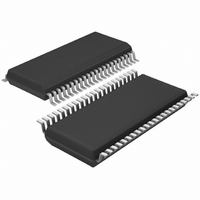
LTC1343CGW#TRPBF Linear Technology, LTC1343CGW#TRPBF Datasheet - Page 5

LTC1343CGW#TRPBF
Manufacturer Part Number
LTC1343CGW#TRPBF
Description
IC TXRX SOFTWARE-SELECTBL 44SSOP
Manufacturer
Linear Technology
Type
Transceiverr
Datasheet
1.LTC1343CGWPBF.pdf
(28 pages)
Specifications of LTC1343CGW#TRPBF
Number Of Drivers/receivers
4/4
Protocol
Multiprotocol
Voltage - Supply
4.75 V ~ 5.25 V
Mounting Type
Surface Mount
Package / Case
44-SSOP
Lead Free Status / RoHS Status
Lead free / RoHS Compliant
Available stocks
Company
Part Number
Manufacturer
Quantity
Price
PIN
V
RS232. Connect a 1 F capacitor to ground.
C1
1 F capacitor between C1
PWRV
4.75V PWRV
with a 1 F capacitor to ground.
temperature range, otherwise specifications are at T
SYMBOL
V.10 Receiver
V
I
R
t
t
t
V.28 Driver
V
I
I
SR
t
t
V.28 Receiver
V
V
R
t
t
t
ELECTRICAL CHARACTERISTICS
Note 1: Absolute Maximum Ratings are those beyond which the safety of a
device may be impaired.
Note 2: All currents into device pins are positive; all currents out of device
are negative. All voltages are referenced to device ground unless otherwise
specified.
IN
SS
OZ
PLH
PHL
PLH
r
PLH
PHL
PHL
r
TH
O
THL
TLH
V
IN
, t
V
IN
, t
DD
TH
TH
+
f
f
U
(Pin 2): Capacitor C1 Positive Terminal. Connect a
(Pin 1): Generated Positive Supply Voltage for
CC
FUNCTIONS
(Pin 3): Positive Supply for the Charge Pump.
U
PARAMETER
Receiver Input Threshold Voltage
Receiver Input Hysteresis
Receiver Input Current
Receiver Input Impedance
Rise or Fall Time
Input to Output
Input to Output
Output Voltage
Short-Circuit Current
Output Leakage Current
Slew Rate
Input to Output
Input to Output
Input Low Threshold Voltage
Input High Threshold Voltage
Receiver Input Hysteresis
Receiver Input Impedance
Rise or Fall Time
Input to Output
Input to Output
CC
5.25V. Tie to V
U
+
and C1
CC
–
.
(Pin 8) and bypass
A
CONDITIONS
0 C T
–7V V
– 10V V
– 10V V
(Figures 5, 9)
(Figures 5, 9)
(Figures 5, 9)
Open Circuit
R
V
– 0.25V V
No-Cable Mode or Driver Disabled
(Figures 4, 8), R
(Figures 4, 8), R
(Figures 4, 8), R
– 15V V
(Figures 5, 9)
(Figures 5, 9), CTRL = 0V
CTRL = V
(Figures 5, 9), CTRL = 0V
CTRL = V
= 25 C. V
O
L
= 3k (Figure 4)
= GND
The
A
CM
CC
CC
A
A
A
CC
70 C
O
denotes specifications which apply over the full operating
7V, – 40 C T
10V
10V
15V
= 5V (Notes 2, 3)
0.25V, Power Off or
L
L
L
= 3k, C
= 3k, C
= 3k, C
Note 3: All typicals are given for V
C
C1
D1 (Pin 5): TTL Level Driver 1 Input.
D2 (Pin 6): TTL Level Driver 2 Input.
D3 (Pin 7): TTL Level Driver 3 Input. Becomes a CMOS
level output when the chip is in the echoed clock mode
(EC = 0V).
VEE
–
= 3.3 F tantalum capacitors and T
(Pin 4): Capacitor C1 Negative Terminal.
L
L
L
= 2500pF
= 2500pF
= 2500pF
A
85 C
CC
– 0.2
– 0.3
MIN
4.0
2.0
0.1
20
3
= 5V, C1 = C2 = C
5
A
= 25 C.
TYP
350
350
110
330
170
480
7.6
1.6
1.6
1.4
1.4
0.4
0.01
11
30
15
15
5
VCC
LTC1343
MAX
30.0
800
800
0.2
0.3
0.50
2.5
2.5
0.8
1.0
50
150
100
7
10
= C
VDD
= 1 F,
UNITS
5
V/ s
mV
mA
mA
k
k
ns
ns
ns
ns
ns
ns
ns
ns
V
V
V
V
A
V
V
V
s
s


