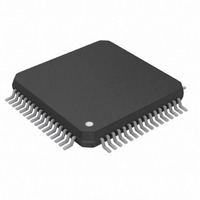
DS26521LN+ Maxim Integrated Products, DS26521LN+ Datasheet - Page 24

DS26521LN+
Manufacturer Part Number
DS26521LN+
Description
IC TXRX T1/E1/J1 64-LQFP
Manufacturer
Maxim Integrated Products
Type
Line Interface Units (LIUs)r
Datasheet
1.DS26521LN.pdf
(258 pages)
Specifications of DS26521LN+
Number Of Drivers/receivers
1/1
Protocol
T1/E1/J1
Voltage - Supply
3.135 V ~ 3.465 V
Mounting Type
Surface Mount
Package / Case
64-LQFP
Lead Free Status / RoHS Status
Lead free / RoHS Compliant
- Current page: 24 of 258
- Download datasheet (2Mb)
SCANMODE
SCAN_EN
ARVDD
ACVDD
ATVDD
ARVSS
ACVSS
ATVSS
JTCLK
NAME
JTRST
DVDD
DVSS
JTMS
JTDO
JTDI
PIN
47
46
45
44
43
12
40
41
21
22
3
4
5
8
9
impedance
I, Pullup
I, Pullup
I, Pullup
O, High
TYPE
—
—
—
—
—
—
—
—
I
I
I
JTAG Reset. JTRST is used to asynchronously reset the test access port
controller. After power-up, JTRST must be toggled from low to high. This action
sets the device into the JTAG DEVICE ID mode. Pulling JTRST low restores
normal device operation. JTRST is pulled high internally via a 10k Ω resistor
operation. If boundary scan is not used, this pin should be held low.
JTAG Mode Select. This pin is sampled on the rising edge of JTCLK and is used
to place the test access port into the various defined IEEE 1149.1 states. This pin
has a 10k Ω pullup resistor.
JTAG Clock. This signal is used to shift data into JTDI on the rising edge and out
of JTDO on the falling edge.
JTAG Data In. Test instructions and data are clocked into this pin on the rising
edge of JTCLK. This pin has a 10k Ω pullup resistor.
JTAG Data Out. Test instructions and data are clocked out of this pin on the falling
edge of JTCLK. If not used, this pin should be left unconnected.
Scan Mode. This pin should be connected to ground for normal operation.
Scan Enable. This pin should be connected to ground for normal operation.
3.3V Analog Transmit Power Supply . This V
section of the DS26521.
Analog Transmit V
3.3V Analog Receive Power Supply . This V
section of the DS26521.
Analog Receive V
Analog Clock Conversion V
unit of the DS26521.
Analog Clock V
3.3V Power Supply for the Digital Framer
Digital Ground for the Framer
POWER SUPPLIES
24 of 258
TEST
SS
. This pin is used for clock converter analog V
SS
SS
. This pin is used for analog V
. This pin is used for transmit analog V
DD
. This V
FUNCTION
DS26521 Single T1/E1/J1 Transceiver
DD
input is used for the clock conversion
DD
DD
input is used for the receive LIU
input is used for the transmit LIU
SS
for the receiver.
SS
.
SS
.
Related parts for DS26521LN+
Image
Part Number
Description
Manufacturer
Datasheet
Request
R

Part Number:
Description:
Ds26521 Single T1/e1/j1 Transceiver
Manufacturer:
Maxim Integrated Products, Inc.
Datasheet:

Part Number:
Description:
power light source LUXEON® Collimator
Manufacturer:
LUMILEDS [Lumileds Lighting Company]
Datasheet:

Part Number:
Description:
MAX7528KCWPMaxim Integrated Products [CMOS Dual 8-Bit Buffered Multiplying DACs]
Manufacturer:
Maxim Integrated Products
Datasheet:

Part Number:
Description:
Single +5V, fully integrated, 1.25Gbps laser diode driver.
Manufacturer:
Maxim Integrated Products
Datasheet:

Part Number:
Description:
Single +5V, fully integrated, 155Mbps laser diode driver.
Manufacturer:
Maxim Integrated Products
Datasheet:

Part Number:
Description:
VRD11/VRD10, K8 Rev F 2/3/4-Phase PWM Controllers with Integrated Dual MOSFET Drivers
Manufacturer:
Maxim Integrated Products
Datasheet:

Part Number:
Description:
Highly Integrated Level 2 SMBus Battery Chargers
Manufacturer:
Maxim Integrated Products
Datasheet:

Part Number:
Description:
Current Monitor and Accumulator with Integrated Sense Resistor; ; Temperature Range: -40°C to +85°C
Manufacturer:
Maxim Integrated Products

Part Number:
Description:
TSSOP 14/A°/RS-485 Transceivers with Integrated 100O/120O Termination Resis
Manufacturer:
Maxim Integrated Products

Part Number:
Description:
TSSOP 14/A°/RS-485 Transceivers with Integrated 100O/120O Termination Resis
Manufacturer:
Maxim Integrated Products

Part Number:
Description:
QFN 16/A°/AC-DC and DC-DC Peak-Current-Mode Converters with Integrated Step
Manufacturer:
Maxim Integrated Products

Part Number:
Description:
TDFN/A/65V, 1A, 600KHZ, SYNCHRONOUS STEP-DOWN REGULATOR WITH INTEGRATED SWI
Manufacturer:
Maxim Integrated Products

Part Number:
Description:
Integrated Temperature Controller f
Manufacturer:
Maxim Integrated Products

Part Number:
Description:
SOT23-6/I°/45MHz to 650MHz, Integrated IF VCOs with Differential Output
Manufacturer:
Maxim Integrated Products


