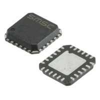
USB3311C-CP-TR SMSC, USB3311C-CP-TR Datasheet - Page 6

USB3311C-CP-TR
Manufacturer Part Number
USB3311C-CP-TR
Description
TXRX USB ULPI 26MHZ CLK 24QFN
Manufacturer
SMSC
Series
flexPWR™r
Type
USB Transceiverr
Specifications of USB3311C-CP-TR
Protocol
USB 2.0
Voltage - Supply
1.6 V ~ 3.6 V
Mounting Type
Surface Mount
Package / Case
24-QFN
Operating Supply Voltage
3.3 V
Mounting Style
SMD/SMT
Operating Temperature Range
- 40 C to + 85 C
For Use With
638-1096 - EVALUATION BOARD FOR USB3311C
Number Of Drivers/receivers
-
Lead Free Status / Rohs Status
Lead free / RoHS Compliant
Other names
638-1091-2
USB3311C-CP
USB3311C-CP
Available stocks
Company
Part Number
Manufacturer
Quantity
Price
Company:
Part Number:
USB3311C-CP-TR
Manufacturer:
SMSC
Quantity:
4 000
Revision 2.1 (06-10-10)
Pin Definitions
BALL
PIN/
B1
C1
C2
D2
D1
D3
D4
D5
C4
E1
E2
E3
10
E4
12
E5
13
14
11
1
2
3
4
5
6
7
8
9
The following table details the pin definitions for the figure above.
SPKR_R/M
CLKOUT
SPKR_L
DATA[7]
DATA[6]
DATA[5]
DATA[4]
DATA[3]
VDD3.3
NAME
VBUS
VBAT
DM
DP
ID
Table 1 USB3311 Pin Description
PRODUCT PREVIEW
DIRECTION/
Hi-Speed USB Transceiver with 1.8V ULPI Interface - 26MHz Reference Clock
Output,
Analog
Analog
Analog
Analog
Analog
Analog
CMOS
CMOS
CMOS
CMOS
CMOS
CMOS
Power
Power
TYPE
Input,
I/O,
I/O,
I/O,
I/O,
I/O,
I/O,
I/O,
I/O,
I/O,
I/O,
6
ACTIVE
LEVEL
N/A
N/A
N/A
N/A
N/A
N/A
N/A
N/A
N/A
N/A
N/A
N/A
N/A
N/A
ID pin of the USB cable. For non-OTG
applications this pin can be floated. For
an A-Device ID is grounded. For a B-
Device ID is floated.
VBUS pin of the USB cable. This pin is
used for the Vbus comparator inputs and
for Vbus pulsing during session request
protocol.
Regulator input. The regulator supply can
be from 5.5V to 3.1V.
3.3V Regulator Output. A 2.2uF (<1 ohm
ESR) bypass capacitor to ground is
required for regulator stability. The
bypass capacitor should be placed as
close as possible to the USB3311.
D- pin of the USB cable.
D+ pin of the USB cable.
USB switch in/out for DP signals
USB switch in/out for DM signals
ULPI bi-directional data bus. DATA[7] is
the MSB.
ULPI bi-directional data bus.
ULPI bi-directional data bus.
ULPI bi-directional data bus.
60MHz reference clock output. All ULPI
signals are driven synchronous to the
rising edge of this clock.
The system must not drive voltage on the
CLKOUT pin following POR or hardware
reset that exceeds the value of V
ULPI bi-directional data bus.
DESCRIPTION
SMSC USB3311 REV C
IH_ED
.


