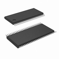
DS90CR287MTD/NOPB National Semiconductor, DS90CR287MTD/NOPB Datasheet - Page 14

DS90CR287MTD/NOPB
Manufacturer Part Number
DS90CR287MTD/NOPB
Description
IC TX 28BIT CHAN LINK 56TSSOP
Manufacturer
National Semiconductor
Type
Driverr
Datasheet
1.DS90CR287MTDNOPB.pdf
(16 pages)
Specifications of DS90CR287MTD/NOPB
Number Of Drivers/receivers
3/0
Protocol
RS644
Voltage - Supply
3 V ~ 3.6 V
Mounting Type
Surface Mount
Package / Case
56-TSSOP
Supply Current
60mA
Supply Voltage Range
3V To 3.6V
Driver Case Style
TSSOP
No. Of Pins
56
Operating Temperature Range
-10°C To +70°C
Msl
MSL 2 - 1 Year
Device Type
Line
Filter Terminals
SMD
Rohs Compliant
Yes
Esd Hbm
7kV
Lead Free Status / RoHS Status
Lead free / RoHS Compliant
Other names
*DS90CR287MTD
*DS90CR287MTD/NOPB
DS90CR287MTD
*DS90CR287MTD/NOPB
DS90CR287MTD
Available stocks
Company
Part Number
Manufacturer
Quantity
Price
Company:
Part Number:
DS90CR287MTD/NOPB
Manufacturer:
PIONEER
Quantity:
560
www.national.com
Applications Information
ramic type in surface mount form factor) between each V
and the ground plane(s) are recommended. The three ca-
pacitor values are 0.1 µF, 0.01 µF and 0.001 µF. An example
is shown in Figure 18. The designer should employ wide
CLOCK JITTER: The CHANNEL LINK devices employ a
PLL to generate and recover the clock transmitted across the
LVDS interface. The width of each bit in the serialized LVDS
data stream is one-seventh the clock period. For example, a
85 MHz clock has a period of 11.76 ns which results in a data
bit width of 1.68 ns. Differential skew (∆t within one differen-
tial pair), interconnect skew (∆t of one differential pair to
another) and clock jitter will all reduce the available window
for sampling the LVDS serial data streams. Care must be
taken to ensure that the clock input to the transmitter be a
clean low noise signal. Individual bypassing of each V
ground will minimize the noise passed on to the PLL, thus
creating a low jitter LVDS clock. These measures provide
more margin for channel-to-channel skew and interconnect
skew as a part of the overall jitter/skew budget.
INPUT CLOCK: The input clock should be present at all
times when the part in enabled. If the clock is stopped, the
PWR DOWN pin should be asserted to disable the PLL.
Once the clock is active again, the part can then be enabled.
Do not enable the part without a clock present.
COMMON-MODE vs. DIFFERENTIAL MODE NOISE MAR-
GIN: The typical signal swing for LVDS is 300 mV centered
at +1.2V. The CHANNEL LINK receiver supports a 100 mV
threshold therefore providing approximately 200 mV of dif-
ferential noise margin. Common-mode protection is of more
importance to the system’s operation due to the differential
FIGURE 17. LVDS Serialized Link Termination
(Continued)
FIGURE 18. CHANNEL LINK
Decoupling Configuration
CC
CC
to
14
traces for power and ground and ensure each capacitor has
its own via to the ground plane. If board space is limiting the
number of bypass capacitors, the PLL V
the most filtering/bypassing. Next would be the LVDS V
pins and finally the logic V
data transmission. LVDS supports an input voltage range of
Ground to +2.4V. This allows for a
center point due to ground potential differences and
common-mode noise.
TRANSMITTER INPUT CLOCK: The transmitter input clock
must always be present when the device is enabled (PWR
DOWN = HIGH). If the clock is stopped, the PWR DOWN pin
must be used to disable the PLL. The PWR DOWN pin must
be held low until after the input clock signal has been reap-
plied. This will ensure a proper device reset and PLL lock to
occur.
POWER SEQUENCING AND POWERDOWN MODE: Out-
puts of the CHANNEL LINK transmitter remain in TRI-STATE
until the power supply reaches 2V. Clock and data outputs
will begin to toggle 10 ms after V
Powerdown pin is above 1.5V. Either device may be placed
into a powerdown mode at any time by asserting the Pow-
erdown pin (active low). Total power dissipation for each
device will decrease to 5 µW (typical).
The transmitter input clock may be applied prior to powering
up and enabling the transmitter. The transmitter input clock
may also be applied after power up; however, the use of the
PWR DOWN pin is required as described in the Transmitter
10108725
CC
pins.
CC
has reached 3V and the
±
1.0V shifting of the
CC
10108724
should receive
CC


