DS90CR287MTD/NOPB National Semiconductor, DS90CR287MTD/NOPB Datasheet - Page 13
DS90CR287MTD/NOPB
Manufacturer Part Number
DS90CR287MTD/NOPB
Description
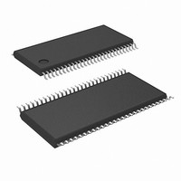
IC TX 28BIT CHAN LINK 56TSSOP
Manufacturer
National Semiconductor
Type
Driverr
Datasheet
1.DS90CR287MTDNOPB.pdf
(16 pages)
Specifications of DS90CR287MTD/NOPB
Number Of Drivers/receivers
3/0
Protocol
RS644
Voltage - Supply
3 V ~ 3.6 V
Mounting Type
Surface Mount
Package / Case
56-TSSOP
Supply Current
60mA
Supply Voltage Range
3V To 3.6V
Driver Case Style
TSSOP
No. Of Pins
56
Operating Temperature Range
-10°C To +70°C
Msl
MSL 2 - 1 Year
Device Type
Line
Filter Terminals
SMD
Rohs Compliant
Yes
Esd Hbm
7kV
Lead Free Status / RoHS Status
Lead free / RoHS Compliant
Other names
*DS90CR287MTD
*DS90CR287MTD/NOPB
DS90CR287MTD
*DS90CR287MTD/NOPB
DS90CR287MTD
Available stocks
Company
Part Number
Manufacturer
Quantity
Price
Company:

Part Number:
DS90CR287MTD/NOPB
Manufacturer:
PIONEER
Quantity:
560


Applications Information
The TSSOP version of the DS90CR287 and DS90CR288A
are backward compatible with the existing 5V Channel Link
transmitter/receiver pair (DS90CR283, DS90CR284). To up-
grade from a 5V to a 3.3V system the following must be
addressed:
1. Change 5V power supply to 3.3V. Provide this supply to
2. Transmitter input and control inputs except 3.3V TTL/
3. The receiver powerdown feature when enabled will lock
The Channel Link devices are intended to be used in a wide
variety of data transmission applications. Depending upon
the application the interconnecting media may vary. For
example, for lower data rate (clock rate) and shorter cable
lengths (
critical. For higher speed/long distance applications the me-
dia’s performance becomes more critical. Certain cable con-
structions provide tighter skew (matched electrical length
between the conductors and pairs). Additional applications
information can be found in the following National Interface
Application Notes:
CABLES: A cable interface between the transmitter and
receiver needs to support the differential LVDS pairs. The
21-bit CHANNEL LINK chipset (DS90CR217/218A) requires
four pairs of signal wires and the 28-bit CHANNEL LINK
chipset (DS90CR287/288A) requires five pairs of signal
wires. The ideal cable/connector interface would have a
constant 100Ω differential impedance throughout the path. It
is also recommended that cable skew remain below 140ps
(
window at the receiver.
In addition to the four or five cable pairs that carry data and
clock, it is recommended to provide at least one additional
conductor (or pair) which connects ground between the
transmitter and receiver. This low impedance ground pro-
vides a common-mode return path for the two devices.
Some of the more commonly used cable types for point-to-
point applications include flat ribbon, flex, twisted pair and
Twin-Coax. All are available in a variety of configurations and
options. Flat ribbon cable, flex and twisted pair generally
perform well in short point-to-point applications while Twin-
Coax is good for short and long applications. When using
ribbon cable, it is recommended to place a ground line
between each differential pair to act as a barrier to noise
coupling between adjacent pairs. For Twin-Coax cable ap-
plications, it is recommended to utilize a shield on each
cable pair. All extended point-to-point applications should
also employ an overall shield surrounding all cable pairs
regardless of the cable type. This overall shield results in
improved transmission parameters such as faster attainable
speeds, longer distances between transmitter and receiver
and reduced problems associated with EMS or EMI.
AN-1041
AN-1108
AN-806
AN-905
AN-916
@
AN = ####
85 MHz clock rate) to maintain a sufficient data sampling
the V
CMOS levels. They are not 5V tolerant.
receiver output to a logic low.
<
CC
, LVDS V
2m), the media electrical performance is less
Introduction to Channel Link
Channel Link PCB and Interconnect
Design-In Guidelines
Transmission Line Theory
Transmission Line Calculations and
Differential Impedance
Cable Information
CC
and PLL V
Topic
CC
.
13
The high-speed transport of LVDS signals has been demon-
strated on several types of cables with excellent results.
However, the best overall performance has been seen when
using Twin-Coax cable. Twin-Coax has very low cable skew
and EMI due to its construction and double shielding. All of
the design considerations discussed here and listed in the
supplemental application notes provide the subsystem com-
munications designer with many useful guidelines. It is rec-
ommended that the designer assess the tradeoffs of each
application thoroughly to arrive at a reliable and economical
cable solution.
RECEIVER FAILSAFE FEATURE: These receivers have
input failsafe bias circuitry to guarantee a stable receiver
output for floating or terminated receiver inputs. Under these
conditions receiver inputs will be in a HIGH state. If a clock
signal is present, data outputs will all be HIGH; if the clock
input is also floating/terminated, data outputs will remain in
the last valid state. A floating/terminated clock input will
result in a HIGH clock output.
BOARD LAYOUT: To obtain the maximum benefit from the
noise and EMI reductions of LVDS, attention should be paid
to the layout of differential lines. Lines of a differential pair
should always be adjacent to eliminate noise interference
from other signals and take full advantage of the noise
canceling of the differential signals. The board designer
should also try to maintain equal length on signal traces for
a given differential pair. As with any high-speed design, the
impedance discontinuities should be limited (reduce the
numbers of vias and no 90 degree angles on traces). Any
discontinuities which do occur on one signal line should be
mirrored in the other line of the differential pair. Care should
be taken to ensure that the differential trace impedance
match the differential impedance of the selected physical
media (this impedance should also match the value of the
termination resistor that is connected across the differential
pair at the receiver’s input). Finally, the location of the
CHANNEL LINK TxOUT/RxIN pins should be as close as
possible to the board edge so as to eliminate excessive pcb
runs. All of these considerations will limit reflections and
crosstalk which adversely effect high frequency performance
and EMI.
INPUTS: The TxIN and control pin inputs are compatible
with LVTTL and LVCMOS levels. This pins are not 5V toler-
ant.
UNUSED INPUTS: All unused inputs at the TxIN inputs of
the transmitter may be tied to ground or left no connect. All
unused outputs at the RxOUT outputs of the receiver must
then be left floating.
TERMINATION: Use of current mode drivers requires a
terminating resistor across the receiver inputs. The CHAN-
NEL LINK chipset will normally require a single 100Ω resistor
between the true and complement lines on each differential
pair of the receiver input. The actual value of the termination
resistor should be selected to match the differential mode
characteristic impedance (90Ω to 120Ω typical) of the cable.
Figure 17 shows an example. No additional pull-up or pull-
down resistors are necessary as with some other differential
technologies such as PECL. Surface mount resistors are
recommended to avoid the additional inductance that ac-
companies leaded resistors. These resistors should be
placed as close as possible to the receiver input pins to
reduce stubs and effectively terminate the differential lines.
DECOUPLING CAPACITORS: Bypassing capacitors are
needed to reduce the impact of switching noise which could
limit performance. For a conservative approach three
parallel-connected decoupling capacitors (Multi-Layered Ce-
www.national.com
Related parts for DS90CR287MTD/NOPB
Image
Part Number
Description
Manufacturer
Datasheet
Request
R

Part Number:
Description:
National Semiconductor [8-Bit D/A Converter]
Manufacturer:
National Semiconductor
Datasheet:
Part Number:
Description:
National Semiconductor [Media Coprocessor]
Manufacturer:
National Semiconductor
Datasheet:
Part Number:
Description:
Digitally Controlled Tone and Volume Circuit with Stereo Audio Power Amplifier, Microphone Preamp Stage and National 3D Sound
Manufacturer:
National Semiconductor
Datasheet:
Part Number:
Description:
Digitally Controlled Tone and Volume Circuit with Stereo Audio Power Amplifier, Microphone Preamp Stage and National 3D Sound
Manufacturer:
National Semiconductor
Datasheet:
Part Number:
Description:
AC97 Rev 2 Codec with Sample Rate Conversion and National 3D Sound
Manufacturer:
National Semiconductor
Part Number:
Description:
Manufacturer:
National Semiconductor
Datasheet:
Part Number:
Description:
Manufacturer:
National Semiconductor
Datasheet:
Part Number:
Description:
General Purpose, Low Voltage, Low Power, Rail-to-Rail Output Operational Amplifiers
Manufacturer:
National Semiconductor
Datasheet:
Part Number:
Description:
8-bit 20 MSPS flash A/D converter.
Manufacturer:
National Semiconductor
Datasheet:
Part Number:
Description:
Low Noise Quad Operational Amplifier
Manufacturer:
National Semiconductor
Datasheet:
Part Number:
Description:
Quad Differential Line Receivers
Manufacturer:
National Semiconductor
Datasheet:
Part Number:
Description:
Quad High Speed Trapezoidal? Bus Transceiver
Manufacturer:
National Semiconductor
Datasheet:
Part Number:
Description:
Dual Line Receiver
Manufacturer:
National Semiconductor
Datasheet:
Part Number:
Description:
TTL to 10k ECL Level Translator with Latch
Manufacturer:
National Semiconductor
Datasheet: