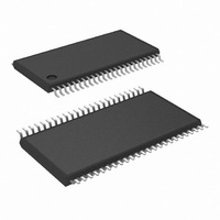
DS90CF364AMTD/NOPB National Semiconductor, DS90CF364AMTD/NOPB Datasheet - Page 4

DS90CF364AMTD/NOPB
Manufacturer Part Number
DS90CF364AMTD/NOPB
Description
IC RCVR LVDS FPD 18BIT 48-TSSOP
Manufacturer
National Semiconductor
Type
Driverr
Datasheets
1.DS90CF364AMTDNOPB.pdf
(14 pages)
2.DS90CF364MTD.pdf
(16 pages)
3.DS90CF364MTDNOPB.pdf
(16 pages)
Specifications of DS90CF364AMTD/NOPB
Number Of Drivers/receivers
1/0
Protocol
RS644
Voltage - Supply
3 V ~ 3.6 V
Mounting Type
Surface Mount
Package / Case
48-TSSOP
Number Of Drivers
21
Number Of Receivers
3
Data Rate
1300 Mbps
Operating Supply Voltage
3.3 V
Maximum Power Dissipation
1890 mW
Maximum Operating Temperature
+ 70 C
Minimum Operating Temperature
- 10 C
Mounting Style
SMD/SMT
Supply Voltage (max)
3.6 V
Supply Voltage (min)
3 V
Supply Current
60mA
Supply Voltage Range
3V To 3.6V
Driver Case Style
TSSOP
No. Of Pins
48
Operating Temperature Range
-10°C To +70°C
Msl
MSL 2 - 1 Year
Bandwidth
170GHz
Rohs Compliant
Yes
Lead Free Status / RoHS Status
Lead free / RoHS Compliant
Other names
*DS90CF364AMTD
*DS90CF364AMTD/NOPB
DS90CF364AMTD
*DS90CF364AMTD/NOPB
DS90CF364AMTD
Available stocks
Company
Part Number
Manufacturer
Quantity
Price
Company:
Part Number:
DS90CF364AMTD/NOPB
Manufacturer:
TI
Quantity:
106
www.national.com
ICCTG
ICCTZ
RECEIVER SUPPLY CURRENT
ICCRW
ICCRG
ICCRZ
LLHT
LHLT
TCIT
TCCS
TPPos0
TPPos1
TPPos2
TPPos3
TPPos4
TPPos5
TPPos6
TCIP
TCIH
TCIL
TSTC
THTC
TCCD
TPLLS
TPDD
Symbol
Symbol
Note 1: “Absolute Maximum Ratings” are those values beyond which the safety of the device cannot be guaranteed. They are not meant to imply that the device
should be operated at these limits. The tables of “Electrical Characteristics” specify conditions for device operation.
Note 2: Typical values are given for V
Note 3: Current into device pins is defined as positive. Current out of device pins is defined as negative. Voltages are referenced to ground unless otherwise
specified (except V
Note 4: V
Transmitter Switching Characteristics
Over recommended operating supply and −40°C to +85°C ranges unless otherwise specified
OS
Transmitter Supply Current, 16 Grayscale R
Transmitter Supply Current
Power Down
Receiver Supply Current, Worst Case
Receiver Supply Current, 16 Grayscale
Receiver Supply Current
Power Down
LVDS Low-to-High Transition Time
LVDS High-to-Low Transition Time
TxCLK IN Transition Time
TxOUT Channel-to-Channel Skew
Transmitter Output Pulse Position for Bit 0
Transmitter Output Pulse Position for Bit 1
Transmitter Output Pulse Position for Bit 2
Transmitter Output Pulse Position for Bit 3
Transmitter Output Pulse Position for Bit 4
Transmitter Output Pulse Position for Bit 5
Transmitter Output Pulse Position for Bit 6
TxCLK IN Period
TxCLK IN High Time
TxCLK IN Low Time
TxIN Setup to TxCLK IN
TxIN Hold to TxCLK IN
TxCLK IN to TxCLK OUT Delay @ 25°C, V
Transmitter Phase Lock Loop Set
Transmitter Power Down Delay
previously referred as V
OD
and ΔV
Parameter
OD
).
(Figure
CM
CC
(Figure
(Figure
.
= 3.3V and T
(Figure 7
(Figure 7
7)
(Figure 5
7)
7)
Parameter
(Figure 15
)
A
(Figure 11
)
= +25C.
(Figure 6
(Figure 3
(Figure 3
)
C
16 Grayscale Pattern
(Figures 2, 3 ), T
to +85°C
PWR DWN = Low
Driver Outputs in TRI-STATE
Power Down Mode
C
Pattern (Figures 1, 4 ),
T
C
Pattern (Figures 2, 4 ),
T
PWR DWN = Low
Receiver Outputs Stay Low during
Power Down Mode
A
A
)
CC
L
L
L
L
(Figure 17
= −40°C to +85°C
= −40°C to +85°C
= 100Ω,
= 5 pF,
= 8 pF, Worst Case
= 8 pF, 16 Grayscale
)
)
)
)
= 3.3V
4
(Figure 9
) f = 65 MHz
f = 65 MHz
Conditions
A
= −40°C
)
f = 32.5 MHz
f = 37.5 MHz
f = 65 MHz
f = 32.5 MHz
f = 37.5 MHz
f = 65 MHz
f = 32.5 MHz
f = 37.5 MHz
f = 65 MHz
®
under
0.35T
0.35T
−0.4
10.6
12.8
Min
1.8
4.0
6.2
8.4
2.5
3.0
15
0
Min
0.75
0.75
11.0
13.2
0.5T
0.5T
Typ
250
2.2
4.4
6.6
8.8
3.7
0
T
Typ
23
28
31
10
49
53
78
28
30
43
10
0.65T
0.65T
Max
11.3
13.5
100
1.5
1.5
0.3
2.5
4.7
6.9
9.1
5.5
50
10
5
Max
105
35
40
45
55
65
70
45
47
60
55
Units
Units
mA
mA
mA
mA
mA
mA
mA
mA
mA
μA
μA
ms
ns
ns
ns
ps
ns
ns
ns
ns
ns
ns
ns
ns
ns
ns
ns
ns
ns
ns


