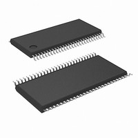
DS90C385AMT/NOPB National Semiconductor, DS90C385AMT/NOPB Datasheet

DS90C385AMT/NOPB
Specifications of DS90C385AMT/NOPB
*DS90C385AMT/NOPB
DS90C385AMT
Available stocks
Related parts for DS90C385AMT/NOPB
DS90C385AMT/NOPB Summary of contents
Page 1
... This chipset is an ideal means to solve EMI and cable size problems associated with wide, high-speed TTL interfaces with added Spread Spectrum Clocking support. Block Diagram © 2006 National Semiconductor Corporation Features n Pin-to-pin compatible to DS90C383, DS90C383A and DS90C385 . n No special start-up sequence required between clock/data and /PD pins ...
Page 2
... Absolute Maximum Ratings If Military/Aerospace specified devices are required, please contact the National Semiconductor Sales Office/ Distributors for availability and specifications. Supply Voltage ( CMOS/TTL Input Voltage LVDS Driver Output Voltage LVDS Output Short Circuit Duration Junction Temperature Storage Temperature Lead Temperature (Soldering, 4 sec) ...
Page 3
Electrical Characteristics Over recommended operating supply and temperature ranges unless otherwise specified. Symbol Parameter TRANSMITTER SUPPLY CURRENT ICCTG Transmitter Supply Current 16 Grayscale ICCTZ Transmitter Supply Current Power Down Note 1: “Absolute Maximum Ratings” are those values beyond which the ...
Page 4
Transmitter Switching Characteristics Over recommended operating supply and temperature ranges unless otherwise specified Symbol TPPos0 Transmitter Output Pulse Position (Figure 12) (Note 5) TPPos1 Transmitter Output Pulse Position TPPos2 Transmitter Output Pulse Position TPPos3 Transmitter Output Pulse Position TPPos4 Transmitter ...
Page 5
Transmitter Switching Characteristics Over recommended operating supply and temperature ranges unless otherwise specified Symbol SSCG Spread Spectrum Clock support; Modulation frequency with a linear profile.(Note 6) TPLLS Transmitter Phase Lock Loop Set (Figure 9) TPDD Transmitter Power Down Delay (Figure ...
Page 6
AC Timing Diagrams FIGURE 2. “16 Grayscale” Test Pattern - DS90C385A (Notes 8, 9, 10) Note 7: The worst case test pattern produces a maximum toggling of digital circuits, LVDS I/O and LVCMOS/LVTTL I/O. Note 8: The 16 grayscale test ...
Page 7
AC Timing Diagrams (Continued) FIGURE 3. DS90C385A (Transmitter) LVDS Output Load. 5pF is showed as board loading FIGURE 4. DS90C385A (Transmitter) LVDS Transition Times FIGURE 5. DS90C385A (Transmitter) Input Clock Transition Time FIGURE 6. DS90C385A (Transmitter) Setup/Hold and High/Low Times ...
Page 8
AC Timing Diagrams FIGURE 8. DS90C385A (Transmitter) Clock In to Clock Out Delay with R_FB pin = GND FIGURE 9. DS90C385A (Transmitter) Phase Lock Loop Set Time FIGURE 10. 28 Parallel TTL Data Inputs Mapped to LVDS Outputs - DS90C385A ...
Page 9
AC Timing Diagrams (Continued) FIGURE 12. Transmitter LVDS Output Pulse Position Measurement - DS90C385A FIGURE 11. Transmitter Power Down Delay 9 20070218 20070226 www.national.com ...
Page 10
DS90C385A MTD56 (TSSOP) Package Pin Descriptions — FPD Link Transmitter Pin Name I/O No. TxIN I 28 LVTTL level input. This includes: 8 Red, 8 Green, 8 Blue, and 4 control lines — FPLINE, FPFRAME and DRDY (also referred to ...
Page 11
Pin Diagram for TSSOP Packages Applications Information The DS90C385A is backward compatible DS90C385, DS90C383A, DS90C383 in TSSOP 56-lead package, and pin-for-pin replacements. This device DS90C385A also features reduced variation of the TCCD parameter which is important for ...
Page 12
Typical Application Truth Table www.national.com TABLE 1. Programmable Transmitter (DS90C385A) Pin Condition Strobe Status R_FB R_FB = V Rising edge strobe CC R_FB R_FB = GND or NC Falling edge strobe 12 20070203 ...
Page 13
... BANNED SUBSTANCE COMPLIANCE National Semiconductor manufactures products and uses packing materials that meet the provisions of the Customer Products Stewardship Specification (CSP-9-111C2) and the Banned Substances and Materials of Interest Specification (CSP-9-111S2) and contain no ‘‘Banned Substances’’ as defined in CSP-9-111S2. ...


