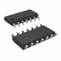
DS90LV019TM/NOPB National Semiconductor, DS90LV019TM/NOPB Datasheet - Page 7

DS90LV019TM/NOPB
Manufacturer Part Number
DS90LV019TM/NOPB
Description
IC DRIVER/RECEIVER LVDS 14-SOIC
Manufacturer
National Semiconductor
Type
Transceiverr
Datasheet
1.DS90LV019TMTCNOPB.pdf
(10 pages)
Specifications of DS90LV019TM/NOPB
Number Of Drivers/receivers
1/1
Protocol
LVDS
Voltage - Supply
3 V ~ 5.5 V
Mounting Type
Surface Mount
Package / Case
14-SOIC (3.9mm Width), 14-SOL
Supply Current
48mA
Supply Voltage Range
3V To 3.6V
Driver Case Style
SOIC
No. Of Pins
8
Operating Temperature Range
-40°C To +85°C
Msl
MSL 1 - Unlimited
Data Rate Max
100Mbps
Rohs Compliant
Yes
Lead Free Status / RoHS Status
Lead free / RoHS Compliant
Other names
*DS90LV019TM
*DS90LV019TM/NOPB
DS90LV019TM
*DS90LV019TM/NOPB
DS90LV019TM
Available stocks
Company
Part Number
Manufacturer
Quantity
Price
Company:
Part Number:
DS90LV019TM/NOPB
Manufacturer:
TI
Quantity:
1 500
Company:
Part Number:
DS90LV019TM/NOPB
Manufacturer:
National Semiconductor
Quantity:
1 983
Test Circuits and Timing Waveforms
Typical Application Diagram
Applications Information
The DS90LV019 has two control pins, which allows the de-
vice to operate as a driver, a receiver or both driver and a re-
ceiver at the same time. There are a few common practices
which should be implied when designing PCB for LVDS sig-
naling. Recommended practices are:
• Use at least 4 PCB board layer (LVDS signals, ground,
• Keep drivers and receivers as close to the (LVDS port
• Bypass each LVDS device and also use distributed bulk
power and TTL signals).
side) connector as possible.
capacitance. Surface mount capacitors placed close to
power and ground pins work best. Two or three multi-
layer ceramic (MLC) surface mount capacitors 0.1 µF,
FIGURE 9. Receiver TRI-STATE Delay Waveforms TRI-STATE Delay Waveforms
FIGURE 10. Terminated Input Fail-Safe Circuit
(Continued)
7
MEDIA (CABLE AND CONNECTOR) SELECTION:
• Use controlled impedance traces which match the differ-
• Use the termination resistor which best matches the dif-
• Isolate TTL signals from LVDS signals.
• Use controlled impedance media. The cables and con-
and 0.01 µF in parallel should be used between each V
and ground. The capacitors should be as close as pos-
sible to the V
ential impedance of your transmission medium (i.e.,
Cable) and termination resistor.
ferential impedance of your transmission line.
nectors should have a matched differential impedance of
about 100 .
DS100053-13
CC
pin.
DS100053-11
DS100053-12
www.national.com
CC


