DS90LV019TM/NOPB National Semiconductor, DS90LV019TM/NOPB Datasheet - Page 2
DS90LV019TM/NOPB
Manufacturer Part Number
DS90LV019TM/NOPB
Description
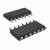
IC DRIVER/RECEIVER LVDS 14-SOIC
Manufacturer
National Semiconductor
Type
Transceiverr
Datasheet
1.DS90LV019TMTCNOPB.pdf
(10 pages)
Specifications of DS90LV019TM/NOPB
Number Of Drivers/receivers
1/1
Protocol
LVDS
Voltage - Supply
3 V ~ 5.5 V
Mounting Type
Surface Mount
Package / Case
14-SOIC (3.9mm Width), 14-SOL
Supply Current
48mA
Supply Voltage Range
3V To 3.6V
Driver Case Style
SOIC
No. Of Pins
8
Operating Temperature Range
-40°C To +85°C
Msl
MSL 1 - Unlimited
Data Rate Max
100Mbps
Rohs Compliant
Yes
Lead Free Status / RoHS Status
Lead free / RoHS Compliant
Other names
*DS90LV019TM
*DS90LV019TM/NOPB
DS90LV019TM
*DS90LV019TM/NOPB
DS90LV019TM
Available stocks
Company
Part Number
Manufacturer
Quantity
Price
Company:

Part Number:
DS90LV019TM/NOPB
Manufacturer:
TI
Quantity:
1 500
Company:
Part Number:
DS90LV019TM/NOPB
Manufacturer:
National Semiconductor
Quantity:
1 983


www.national.com
DIFFERENTIAL DRIVER CHARACTERISTICS
V
V
I
I
I
DIFFERENTIAL RECEIVER CHARACTERISTICS
V
V
I
V
V
I
DEVICE CHARACTERISTICS
V
V
I
I
V
I
I
I
I
C
C
Symbol
OZD
OXD
OSD
OS
IN
IH
IL
CCD
CCR
CCZ
CC
T
DC Electrical Characteristics
V
V
OD
OS
OH
OL
TH
TH
IH
IL
CL
Absolute Maximum Ratings
If Military/Aerospace specified devices are required,
please contact the National Semiconductor Sales Office/
Distributors for availability and specifications.
D output
R input
Supply Voltage V
Enable Input Voltage (DE, RE)
Driver Input Voltage (D
Receiver Output Voltage
Driver Output Voltage (DO
Receiver Input Voltage (RI
Driver Short Circuit Current
ESD (Note 4)
Maximum Package Power Dissipation at 25˚C
A
OD
OS
= −40˚C to +85˚C unless otherwise noted, V
(R
SOIC
(HBM, 1.5 k , 100 pF)
(EIAJ, 0
OUT
)
Output Differential Voltage
V
Offset Voltage
Offset Magnitude Change
TRI-STATE
Power-Off Leakage
Output Short Circuit Current
Voltage Output High
Voltage Output Low
Output Short Circuit Current
Input Threshold High
Input Threshold Low
Input Current
Minimum Input High Voltage
Maximum Input Low Voltage
Input High Current
Input Low Current
Input Diode Clamp Voltage
Power Supply Current
Capacitance
Capacitance
OD
, 200 pF)
Magnitude Change
CC
Parameter
®
Leakage
IN
)
±
±
)
)
−0.3V to (V
−0.3V to (V
−0.3V to (V
−0.3V to (V
R
V
V
V
VID = +100 mV
Inputs Open
I
V
V
0V
V
V
I
DE = RE = V
DE = RE = 0V
DE = 0V, RE = V
DE = V
−0.3V to +3.9V
OL
CLAMP
L
OUT
OUT
OUT
OUT
IN
IN
IN
(Note 1)
CC
= 100
= 2.0 mA, VID = −100 mV
= +2.4V or 0V, V
= V
= GND or 0.4V
Continuous
CC
CC
CC
CC
= V
= 3.6V or GND, V
= 0V, DE = V
= 0V
= 3.3
>
>
960 mW
= −18 mA
CC
CC
+ 0.3V)
+ 0.3V)
+ 0.3V)
+0.3V)
2.0 kV
CC
200 V
, RE = 0V
or 2.4V
6.0V
( Figure 1 )
±
Conditions
or GND, DE = 0V
CC
0.3V. (Notes 2, 3)
CC
2
I
CC
OH
CC
Recommended Operating
Conditions
= −400 µA
Supply Voltage (V
Supply Voltage (V
Receiver Input Voltage
Operating Free Air
CC
Storage Temperature Range
Lead Temperature
= 3.6V or
Temperature T
Derate SOIC Package
TSSOP
Derate TSSOP Package
(Soldering, 4 sec.)
= 0V
DE, RE
DO+,
DO−
A
R
DO+,
DO−
RI+,
D
V
RI+,
CC
CC
Pin
RI−
RI−
OUT
IN
CC
) or
)
,
−100
GND
−1.5
Min
250
−10
−10
−10
−75
−10
2.9
2.9
2.0
1
1.25
−0.7
Typ
350
−34
3.3
3.3
0.1
4.5
3.7
Min
−40
±
±
±
±
±
−6
15
3.0
4.5
0.0
6
5
9
5
5
1
1
1
1
1
−65˚C to +150˚C
Max
+85
+100
3.6
5.5
2.4
Max
12.5
V
450
+10
+10
−20
+10
±
±
1.7
0.4
0.8
7.0
7.0
60
60
−4
20
CC
10
10
7.7mW/˚C
6.3mW/˚C
790 mW
Units
260˚C
˚C
V
V
V
Units
mV
mV
mV
mA
mA
mV
mV
mA
mA
mA
mA
µA
µA
µA
µA
µA
pF
pF
V
V
V
V
V
V
V
Related parts for DS90LV019TM/NOPB
Image
Part Number
Description
Manufacturer
Datasheet
Request
R

Part Number:
Description:
National Semiconductor [8-Bit D/A Converter]
Manufacturer:
National Semiconductor
Datasheet:
Part Number:
Description:
National Semiconductor [Media Coprocessor]
Manufacturer:
National Semiconductor
Datasheet:
Part Number:
Description:
Digitally Controlled Tone and Volume Circuit with Stereo Audio Power Amplifier, Microphone Preamp Stage and National 3D Sound
Manufacturer:
National Semiconductor
Datasheet:
Part Number:
Description:
Digitally Controlled Tone and Volume Circuit with Stereo Audio Power Amplifier, Microphone Preamp Stage and National 3D Sound
Manufacturer:
National Semiconductor
Datasheet:
Part Number:
Description:
AC97 Rev 2 Codec with Sample Rate Conversion and National 3D Sound
Manufacturer:
National Semiconductor
Part Number:
Description:
Manufacturer:
National Semiconductor
Datasheet:
Part Number:
Description:
Manufacturer:
National Semiconductor
Datasheet:
Part Number:
Description:
General Purpose, Low Voltage, Low Power, Rail-to-Rail Output Operational Amplifiers
Manufacturer:
National Semiconductor
Datasheet:
Part Number:
Description:
8-bit 20 MSPS flash A/D converter.
Manufacturer:
National Semiconductor
Datasheet:
Part Number:
Description:
Low Noise Quad Operational Amplifier
Manufacturer:
National Semiconductor
Datasheet:
Part Number:
Description:
Quad Differential Line Receivers
Manufacturer:
National Semiconductor
Datasheet:
Part Number:
Description:
Quad High Speed Trapezoidal? Bus Transceiver
Manufacturer:
National Semiconductor
Datasheet:
Part Number:
Description:
Dual Line Receiver
Manufacturer:
National Semiconductor
Datasheet:
Part Number:
Description:
TTL to 10k ECL Level Translator with Latch
Manufacturer:
National Semiconductor
Datasheet: