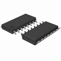
BU2090F-E2 Rohm Semiconductor, BU2090F-E2 Datasheet - Page 8

BU2090F-E2
Manufacturer Part Number
BU2090F-E2
Description
IC DRVR SER/PAR I/O 12BIT SOP16
Manufacturer
Rohm Semiconductor
Type
Driverr
Specifications of BU2090F-E2
Voltage - Supply
2.7 V ~ 5.5 V
Mounting Type
Surface Mount
Package / Case
16-SOP
Output Current
25mA
No. Of Outputs
12
Supply Voltage Range
2.7V To 5.5V
Driver Case Style
SOP
No. Of Pins
16
Operating Temperature Range
-40°C To +85°C
Svhc
No SVHC (18-Jun-2010)
Operating
RoHS Compliant
Supply Voltage (max)
5.5 V
Supply Voltage (min)
2.7 V
Supply Current
.025 A
Maximum Operating Temperature
85 C
Mounting Style
SMD/SMT
Minimum Operating Temperature
- 40 C
Output Voltage
5.5 V to 25 V
Base Number
2090
Rohs Compliant
Yes
Lead Free Status / RoHS Status
Lead free / RoHS Compliant
Number Of Drivers/receivers
-
Protocol
-
Lead Free Status / Rohs Status
Lead free / RoHS Compliant
Other names
BU2090F-E2
BU2090F-E2TR
BU2090F-E2TR
Available stocks
Company
Part Number
Manufacturer
Quantity
Price
•
The logic of the DATA pin is sent to the 12-bit shift register on the rising edge of the CLOCK pulse. Subsequently, it
is shifted from Q0 to Q11 for every clock rising edge.
For the BU2090 / F / FS
When the DATA pin is LOW on the CLOCK falling edge, the data does not change its output state. It is only shifted in
the internal shift register. However, when the DATA pin is HIGH, the content of the 12-bit shift register is latched and
is output to the corresponding Q0 to Q11.
8
Standard ICs
Circuit operation
CLOCK
DATA
Q11
Q10
Q9
Q8
Q7
Q6
Q5
Q4
Q3
Q2
Q1
Q0
D11
D10
D9
D8
D7
D6
D5
Fig.3 Operation timing chart
D4
D3
D2
Note 1)
Note 2) Pull-up resistance is connected to the output pin.
D1
D0
indicates unstable output.
BU2090 / BU2090F / BU2090FS /
BU2092 / BU2092F / BU2092FV


