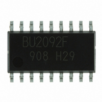
BU2092F-E2 Rohm Semiconductor, BU2092F-E2 Datasheet - Page 6

BU2092F-E2
Manufacturer Part Number
BU2092F-E2
Description
IC DRIVER 12BIT S-IN P-OUT SOP18
Manufacturer
Rohm Semiconductor
Type
Driverr
Specifications of BU2092F-E2
Number Of Drivers/receivers
12/0
Voltage - Supply
2.7 V ~ 5.5 V
Mounting Type
Surface Mount
Package / Case
18-SOP
Output Current
25mA
No. Of Outputs
12
Supply Voltage Range
2.7V To 5.5V
Driver Case Style
SOP
No. Of Pins
18
Operating Temperature Range
-20°C To +75°C
Svhc
No SVHC (18-Jun-2010)
Base
RoHS Compliant
Supply Voltage (max)
5.5 V
Supply Voltage (min)
2.7 V
Supply Current
0.025 A
Maximum Operating Temperature
+ 75 C
Mounting Style
SMD/SMT
Minimum Operating Temperature
- 25 C
Output Voltage
2 V to 1 V
Base Number
2092
Rohs Compliant
Yes
Lead Free Status / RoHS Status
Lead free / RoHS Compliant
Protocol
-
Lead Free Status / Rohs Status
Lead free / RoHS Compliant
Other names
BU2092F-E2TR
Available stocks
Company
Part Number
Manufacturer
Quantity
Price
Part Number:
BU2092F-E2
Manufacturer:
ROHM/罗姆
Quantity:
20 000
●Operating description
●Application circuit
●Interfaces
© 2009 ROHM Co., Ltd. All rights reserved.
BU2050F,BU2092F,BU2092FV,BU2099FV,BD7851FP,BU2152FS
www.rohm.com
INPUT
IN
(1) Data clear
(2) Data transfer
(3) Cascade connection
DATA, CLOCK, STB, CLR
DATA, CLOCK, LCK, OE
GND(VSS)
GND(VSS)
V
When the reset terminal (CLR, CLB) is set to “L”, the content of all latch circuits are set to “H”, and all parallel outputs are
initialised.
Serial data is sequentially input to the shift register during the rise of the clock time (strobe signal is not active). When
the strobe signal is active, the content of the shift register are transferred to the latch circuit.
Serial input data is output from the serial output through the shift register, regardless of the strobe signal.
DD
VSS
V
DD
BU2099FV
BU2152FS
BU2050F
P1~P28
V
DD
(only OE pin)
GND(VSS)
VSS
V
DD
MPU
VDD
VSS
GND(VSS)
V
VSS
DD
GND(VSS)
V
C1
DD
(*)
GND(VSS)
GND(VSS)
V
V
DD
VDD
Serial data input
Clock input
Strobe input
Latch input
VDD
Serial data input
Clock input
Strobe input
Latch input
DD
GND(VSS)
BU2099FV
BU2152FS
BU2050F
Q0~Q11
P1~P8
GND(VSS) GND(VSS)
SO
V
DD
GND(VSS)
P1 P2
P1 P2
OUT
V
DD
OUTPUT
(*C1 must be placed as close to the terminal as possible.)
6/24
IN
DATA, CLOCK, LCK, OE
GND(VSS)
BU2092F/BU2092FV
BU2099FV
V
DD
GND(VSS)
SO
Serial data output
Serial data output
Pn-2 Pn-1 Pn
Pn-2 Pn-1 Pn
V
BU2092F/BU2092FV)
DD
GND(VSS)
(except
(For model with reset terminal only)
OUT
V
VSS
VSS
DD
CLOCK, DATA, STB, CLB
GND(VSS)
BU2092F/BU2092FV
V
DD
for
Technical Note
2009.06 - Rev.A
BU2152FS
Q0~Q11
GND(VSS)
Fig. 1
GND(VSS)
V
DD
BU2050F,
OUT
GND(VSS)
V
DD


