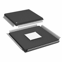
AD9910BSVZ Analog Devices Inc, AD9910BSVZ Datasheet - Page 6

AD9910BSVZ
Manufacturer Part Number
AD9910BSVZ
Description
IC DDS 1GSPS 14BIT PAR 100TQFP
Manufacturer
Analog Devices Inc
Datasheet
1.AD9910BSVZ-REEL.pdf
(64 pages)
Specifications of AD9910BSVZ
Design Resources
Synchronizing Multiple AD9910 1 GSPS Direct Digital Synthesizers (CN0121)
Resolution (bits)
14 b
Master Fclk
1GHz
Tuning Word Width (bits)
32 b
Voltage - Supply
1.8V, 3.3V
Operating Temperature
-40°C ~ 85°C
Mounting Type
Surface Mount
Package / Case
100-TQFP Exposed Pad, 100-eTQFP, 100-HTQFP, 100-VQFP
Pll Type
Frequency Synthesis
Frequency
1GHz
Supply Current
29mA
Supply Voltage Range
1.71V To 1.89V
Digital Ic Case Style
TQFP
No. Of Pins
100
Operating Temperature Range
-40°C To +85°C
Lead Free Status / RoHS Status
Lead free / RoHS Compliant
For Use With
AD9910/PCBZ - BOARD EVAL FOR AD9910 1GSPS
Lead Free Status / RoHS Status
Lead free / RoHS Compliant, Lead free / RoHS Compliant
Available stocks
Company
Part Number
Manufacturer
Quantity
Price
Company:
Part Number:
AD9910BSVZ
Manufacturer:
AVAGO
Quantity:
1 400
Company:
Part Number:
AD9910BSVZ
Manufacturer:
ADI
Quantity:
509
Company:
Part Number:
AD9910BSVZ
Manufacturer:
Analog Devices Inc
Quantity:
10 000
Part Number:
AD9910BSVZ
Manufacturer:
ADI/亚德诺
Quantity:
20 000
Company:
Part Number:
AD9910BSVZ-REEL
Manufacturer:
Analog Devices Inc
Quantity:
10 000
AD9910
SPECIFICATIONS
ELECTRICAL SPECIFICATIONS
AVDD (1.8 V) and DVDD (1.8 V) = 1.8 V ± 5%, AVDD (3.3 V) = 3.3 V ± 5%, DVDD_I/O (3.3 V) = 3.3 V ± 5%, T = 25°C, R
I
Table 1.
Parameter
REFCLK INPUT CHARACTERISTICS
REFCLK MULTIPLIER VCO CHARACTERISTICS
REFCLK_OUT CHARACTERISTICS
DAC OUTPUT CHARACTERISTICS
OUT
Frequency Range
Input Capacitance
Input Impedance
Duty Cycle
REFCLK Input Level
Maximum Capacitive Load
Maximum Frequency
Full-Scale Output Current
Gain Error
Output Offset
Differential Nonlinearity
Integral Nonlinearity
Output Capacitance
Residual Phase Noise
Voltage Compliance Range
Wideband SFDR
Narrow-Band SFDR
External Crystal
VCO Gain (K
= 20 mA, external reference clock frequency = 1000 MHz with reference clock (REFCLK) multiplier disabled, unless otherwise noted.
REFCLK Multiplier
Maximum REFCLK Input Divider Frequency
Minimum REFCLK Input Divider Frequency
REFCLK Multiplier
50.1 MHz Analog Output
101.3 MHz Analog Output
V
) @ Center Frequency
Conditions/Comments
Disabled
Enabled
Full temperature range
Full temperature range
Differential
Single-ended
REFCLK multiplier disabled
REFCLK multiplier enabled
Single-ended
Differential
VCO range Setting 0
VCO range Setting 1
VCO range Setting 2
VCO range Setting 3
VCO range Setting 4
VCO range Setting 5
@ 1 kHz offset, 20 MHz A
Disabled
Enabled @ 20×
Enabled @ 100×
See the Typical Performance
Characteristics section
±500 kHz
±125 kHz
±12.5 kHz
±500 kHz
±125 kHz
±12.5 kHz
Rev. C | Page 6 of 64
1
OUT
Min
100
8.6
−10
−0.5
60
3.2
1500
45
40
50
Typ
1900
25
25
3
2.8
1.4
429
500
555
750
789
850
20
25
20
0.8
1.5
5
−152
−140
−140
–87
–87
–96
–87
–87
–95
Max
1000
60
35
55
60
1000
2000
31.6
+10
2.3
+0.5
MHz
MHz/V
MHz/V
MHz/V
MHz/V
Unit
MHz
MHz
MHz
MHz
pF
kΩ
kΩ
%
%
mV p-p
mV p-p
MHz/V
MHz/V
pF
MHz
mA
% FS
μA
LSB
LSB
pF
dBc/Hz
dBc/Hz
dBc/Hz
V
dBc
dBc
dBc
dBc
dBc
dBc
SET
= 10 kΩ,


