AD9910BSVZ Analog Devices Inc, AD9910BSVZ Datasheet - Page 3
AD9910BSVZ
Manufacturer Part Number
AD9910BSVZ
Description
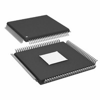
IC DDS 1GSPS 14BIT PAR 100TQFP
Manufacturer
Analog Devices Inc
Datasheet
1.AD9910BSVZ-REEL.pdf
(64 pages)
Specifications of AD9910BSVZ
Design Resources
Synchronizing Multiple AD9910 1 GSPS Direct Digital Synthesizers (CN0121)
Resolution (bits)
14 b
Master Fclk
1GHz
Tuning Word Width (bits)
32 b
Voltage - Supply
1.8V, 3.3V
Operating Temperature
-40°C ~ 85°C
Mounting Type
Surface Mount
Package / Case
100-TQFP Exposed Pad, 100-eTQFP, 100-HTQFP, 100-VQFP
Pll Type
Frequency Synthesis
Frequency
1GHz
Supply Current
29mA
Supply Voltage Range
1.71V To 1.89V
Digital Ic Case Style
TQFP
No. Of Pins
100
Operating Temperature Range
-40°C To +85°C
Lead Free Status / RoHS Status
Lead free / RoHS Compliant
For Use With
AD9910/PCBZ - BOARD EVAL FOR AD9910 1GSPS
Lead Free Status / RoHS Status
Lead free / RoHS Compliant, Lead free / RoHS Compliant
Available stocks
Company
Part Number
Manufacturer
Quantity
Price
Company:

Part Number:
AD9910BSVZ
Manufacturer:
AVAGO
Quantity:
1 400
Company:
Part Number:
AD9910BSVZ
Manufacturer:
ADI
Quantity:
509
Company:
Part Number:
AD9910BSVZ
Manufacturer:
Analog Devices Inc
Quantity:
10 000
Part Number:
AD9910BSVZ
Manufacturer:
ADI/亚德诺
Quantity:
20 000
Company:
Part Number:
AD9910BSVZ-REEL
Manufacturer:
Analog Devices Inc
Quantity:
10 000


Synchronization of Multiple Devices ............................................ 44
Power Supply Partitioning ............................................................. 47
Serial Programming ........................................................................ 48
Power-Down Control ................................................................. 43
3.3 V Supplies .............................................................................. 47
1.8 V Supplies .............................................................................. 47
Control Interface—Serial I/O .................................................... 48
General Serial I/O Operation .................................................... 48
Instruction Byte ........................................................................... 48
Serial I/O Port Pin Descriptions ............................................... 48
DVDD_I/O (3.3 V) (Pin 11, Pin 15, Pin 21, Pin 28, Pin 45,
Pin 56, and Pin 66) .................................................................. 47
AVDD (3.3 V) (Pin 74 to Pin 77 and Pin 83) ...................... 47
DVDD (1.8 V) (Pin 17, Pin 23, Pin 30, Pin 47, Pin 57, and
Pin 64) ...................................................................................... 47
AVDD (1.8 V) (Pin 3)............................................................. 47
AVDD (1.8 V) (Pin 6)............................................................. 47
AVDD (1.8 V) (Pin 89 and Pin 92) ....................................... 47
Instruction Byte Information Bit Map ................................. 48
SCLK—Serial Clock................................................................ 48
CS —Chip Select Bar ............................................................... 48
SDIO—Serial Data Input/Output ......................................... 48
Rev. C | Page 3 of 64
Register Map and Bit Descriptions ............................................... 50
Outline Dimensions ........................................................................ 62
Serial I/O Timing Diagrams ...................................................... 49
MSB/LSB Transfers ..................................................................... 49
Register Bit Descriptions............................................................ 55
Ordering Guide ........................................................................... 62
SDO—Serial Data Out ........................................................... 48
I/O_RESET—Input/Output Reset ........................................ 49
I/O_UPDATE—Input/Output Update ................................ 49
Control Function Register 1 (CFR1)—Address 0x00 ........ 55
Control Function Register 2 (CFR2)—Address 0x01 ........ 57
Control Function Register 3 (CFR3)—Address 0x02 ........ 58
Auxiliary DAC Control Register—Address 0x03 ............... 58
I/O Update Rate Register—Address 0x04 ........................... 59
Frequency Tuning Word Register (FTW)—Address 0x07 ..... 59
Phase Offset Word Register (POW)—Address 0x08 ......... 59
Amplitude Scale Factor Register (ASF)—Address 0x09 .... 59
Multichip Sync Register—Address 0x0A ............................. 60
Digital Ramp Limit Register—Address 0x0B...................... 60
Digital Ramp Step Size Register—Address 0x0C ............... 60
Digital Ramp Rate Register—Address 0x0D ....................... 60
Profile Registers ...................................................................... 61
AD9910
Related parts for AD9910BSVZ
Image
Part Number
Description
Manufacturer
Datasheet
Request
R

Part Number:
Description:
Direct Digital Synthesis Evaluation Board
Manufacturer:
Analog Devices Inc
Datasheet:


Part Number:
Description:
±1.7g Dual-Axis IMEMS Accelerometer Evaluation Board
Manufacturer:
Analog Devices Inc
Datasheet:

Part Number:
Description:
Inertial Sensor Evaluation System
Manufacturer:
Analog Devices Inc
Datasheet:
Part Number:
Description:
Manufacturer:
Analog Devices Inc
Datasheet:
Part Number:
Description:
Manufacturer:
Analog Devices Inc
Datasheet:
Part Number:
Description:
Manufacturer:
Analog Devices Inc
Datasheet:
Part Number:
Description:
Manufacturer:
Analog Devices Inc
Datasheet:
Part Number:
Description:
Manufacturer:
Analog Devices Inc
Datasheet:
Part Number:
Description:
Manufacturer:
Analog Devices Inc
Datasheet:
Part Number:
Description:
Manufacturer:
Analog Devices Inc
Datasheet:
Part Number:
Description:
Manufacturer:
Analog Devices Inc
Datasheet:
Part Number:
Description:
Manufacturer:
Analog Devices Inc
Datasheet: