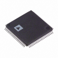
AD9854ASTZ Analog Devices Inc, AD9854ASTZ Datasheet - Page 23

AD9854ASTZ
Manufacturer Part Number
AD9854ASTZ
Description
IC DDS QUADRATURE CMOS 80-LQFP
Manufacturer
Analog Devices Inc
Datasheet
1.AD9854ASTZ.pdf
(52 pages)
Specifications of AD9854ASTZ
Package / Case
80-LQFP
Resolution (bits)
12 b
Master Fclk
300MHz
Tuning Word Width (bits)
48 b
Voltage - Supply
3.14 V ~ 3.47 V
Operating Temperature
-40°C ~ 85°C
Mounting Type
Surface Mount
Supply Voltage Range
3.135V To 3.465V
Operating Temperature Range
-40°C To +85°C
Digital Ic Case Style
LQFP
No. Of Pins
80
Svhc
No SVHC (18-Jun-2010)
Base Number
9854
Ic Function
Direct Digital Synthesizer
Rohs Compliant
Yes
Lead Free Status / RoHS Status
Lead free / RoHS Compliant
For Use With
AD9854/PCBZ - BOARD EVAL FOR AD9854
Lead Free Status / RoHS Status
Lead free / RoHS Compliant, Lead free / RoHS Compliant
Available stocks
Company
Part Number
Manufacturer
Quantity
Price
Company:
Part Number:
AD9854ASTZ
Manufacturer:
Renesas
Quantity:
103
Company:
Part Number:
AD9854ASTZ
Manufacturer:
ADI
Quantity:
271
Company:
Part Number:
AD9854ASTZ
Manufacturer:
Analog Devices Inc
Quantity:
10 000
Part Number:
AD9854ASTZ
Manufacturer:
ADI/亚德诺
Quantity:
20 000
Figure 41 shows that premature toggling causes the ramp to
immediately reverse itself and proceed at the same rate and
resolution until the original frequency is reached.
The control register contains a triangle bit at Parallel Register
Address 1F hex. Setting this bit high in Mode 010 causes an
automatic ramp-up and ramp-down between F1 and F2 to
occur without toggling Pin 29, as shown in Figure 40. The logic
state of Pin 29 has no effect once the triangle bit is set high. This
function uses the ramp rate clock time period and the step size
of the delta frequency word to form a continuously sweeping
linear ramp from F1 to F2 and back to F1 with equal dwell
times at every frequency. Use this function to automatically
sweep between any two frequencies from dc to Nyquist.
In the ramped FSK mode with the triangle bit set high, an
automatic frequency sweep begins at either F1 or F2, according
I/O UD CLK
FSK DATA
MODE
TW1
TW2
000 (DEFAULT)
F2
F1
I/O UD CLK
TRIANGLE
FSK DATA
0
0
0
MODE
TW1
TW2
BIT
Figure 40. Effect of Triangle Bit in Ramped FSK Mode
Figure 41. Effect of Premature Ramped FSK Data
F2
F1
0
Rev. E | Page 23 of 52
010 (RAMPED FSK)
010 (RAMPED FSK)
F1
F2
to the logic level on Pin 29 (FSK input pin) when the triangle
bit’s rising edge occurs (Figure 42). If the FSK data bit is high
instead of low, F2, rather than F1, is chosen as the start frequency.
Additional flexibility in the ramped FSK mode is provided by
the AD9854’s ability to respond to changes in the 48-bit delta
frequency word and/or the 20-bit ramp rate counter at any time
during the ramping from F1 to F2 or vice versa. To create these
nonlinear frequency changes, it is necessary to combine several
linear ramps with different slopes in a piecewise fashion. This is
done by programming and executing a linear ramp at a rate or
slope and then altering the slope (by changing the ramp rate
clock or delta frequency word, or both). Changes in slope can
be made as often as needed before the destination frequency has
been reached to form the desired nonlinear frequency sweep
response. These piecewise changes can be precisely timed using
F2
F1
AD9854


