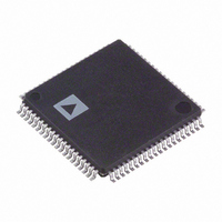
AD9854ASTZ Analog Devices Inc, AD9854ASTZ Datasheet - Page 19

AD9854ASTZ
Manufacturer Part Number
AD9854ASTZ
Description
IC DDS QUADRATURE CMOS 80-LQFP
Manufacturer
Analog Devices Inc
Datasheet
1.AD9854ASTZ.pdf
(52 pages)
Specifications of AD9854ASTZ
Package / Case
80-LQFP
Resolution (bits)
12 b
Master Fclk
300MHz
Tuning Word Width (bits)
48 b
Voltage - Supply
3.14 V ~ 3.47 V
Operating Temperature
-40°C ~ 85°C
Mounting Type
Surface Mount
Supply Voltage Range
3.135V To 3.465V
Operating Temperature Range
-40°C To +85°C
Digital Ic Case Style
LQFP
No. Of Pins
80
Svhc
No SVHC (18-Jun-2010)
Base Number
9854
Ic Function
Direct Digital Synthesizer
Rohs Compliant
Yes
Lead Free Status / RoHS Status
Lead free / RoHS Compliant
For Use With
AD9854/PCBZ - BOARD EVAL FOR AD9854
Lead Free Status / RoHS Status
Lead free / RoHS Compliant, Lead free / RoHS Compliant
Available stocks
Company
Part Number
Manufacturer
Quantity
Price
Company:
Part Number:
AD9854ASTZ
Manufacturer:
Renesas
Quantity:
103
Company:
Part Number:
AD9854ASTZ
Manufacturer:
ADI
Quantity:
271
Company:
Part Number:
AD9854ASTZ
Manufacturer:
Analog Devices Inc
Quantity:
10 000
Part Number:
AD9854ASTZ
Manufacturer:
ADI/亚德诺
Quantity:
20 000
THEORY OF OPERATION
The AD9854 quadrature output digital synthesizer is a highly
flexible device that addresses a wide range of applications. The
device consists of an NCO with a 48-bit phase accumulator, a
programmable reference clock multiplier, inverse sinc filters,
digital multipliers, two 12-bit/300 MHz DACs, a high speed
analog comparator, and interface logic. This highly integrated
device can be configured to serve as a synthesized LO, an agile
clock generator, or an FSK/BPSK modulator.
Analog Devices, Inc., provides a technical tutorial about the
operational theory of the functional blocks of the device. The
tutorial includes a technical description of the signal flow
through a DDS device and provides basic applications
information for a variety of digital synthesis implementations.
The document, A Technical Tutorial on Digital Signal Synthesis,
is available from the DDS Technical Library, on the Analog
Devices DDS website at www.analog.com/dds.
MODES OF OPERATION
The AD9854 has five programmable operational modes. To
select a mode, three bits in the control register (parallel Address
1F hex) must be programmed, as described in Table 5.
Table 5. Mode Selection Table
Mode 2
0
0
0
0
1
Table 6. Functions Available for Modes
Function
Phase Adjust 1
Phase Adjust 2
Single-Pin FSK/BPSK or HOLD
Single-Pin Shaped Keying
Phase Offset or Modulation
Amplitude Control or Modulation
Inverse Sinc Filter
Frequency Tuning Word 1
Frequency Tuning Word 2
Automatic Frequency Sweep
Mode 1
0
0
1
1
0
Mode 0
0
1
0
1
0
Result
Single tone
FSK
Ramped FSK
Chirp
BPSK
Single Tone
Rev. E | Page 19 of 52
●
●
●
●
●
●
In each mode, some functions may be prohibited. Table 6 lists
the functions and their availability for each mode.
Single Tone (Mode 000)
This is the default mode when the MASTER RESET pin is
asserted. It can also be accessed if the user programs this mode
into the control register. The phase accumulator, responsible for
generating an output frequency, is presented with a 48-bit value
from the Frequency Tuning Word 1 registers that have default
values of 0. Default values from the remaining applicable
registers further define the single-tone output signal qualities.
The default values after a master reset configure the device
with an output signal of 0 Hz and zero phase. At power-up and
reset, the output from the I and Q DACs is a dc value equal to
the midscale output current. This is the default mode amplitude
setting of 0. See the On/Off Output Shaped Keying (OSK)
section for more details about the output amplitude control. All
or some of the 28 program registers must be programmed to
produce a user-defined output signal.
Figure 35 shows the transition from the default condition
(0 Hz) to a user-defined output frequency (F1).
FSK
●
●
●
●
●
●
●
●
Ramped FSK
Mode
●
●
●
●
●
●
●
●
●
Chirp
●
●
●
●
●
●
●
●
AD9854
BPSK
●
●
●
●
●
●
●


