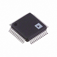
AD9952YSVZ Analog Devices Inc, AD9952YSVZ Datasheet - Page 5

AD9952YSVZ
Manufacturer Part Number
AD9952YSVZ
Description
IC DDS 14BIT DAC 1.8V 48-TQFP
Manufacturer
Analog Devices Inc
Datasheet
1.AD9952YSVZ.pdf
(28 pages)
Specifications of AD9952YSVZ
Resolution (bits)
14 b
Master Fclk
400MHz
Tuning Word Width (bits)
32 b
Voltage - Supply
1.71 V ~ 1.96 V
Operating Temperature
-40°C ~ 105°C
Mounting Type
Surface Mount
Package / Case
48-TQFP Exposed Pad, 48-eTQFP, 48-HTQFP, 48-VQFP
Pll Type
Frequency Synthesis
Frequency
400MHz
Supply Voltage Range
1.71V To 1.89V
Digital Ic Case Style
TQFP
No. Of Pins
48
Operating Temperature Range
-40°C To +105°C
Msl
MSL 3 - 168 Hours
Lead Free Status / RoHS Status
Lead free / RoHS Compliant
For Use With
AD9952/PCB - BOARD EVAL FOR AD9952
Lead Free Status / RoHS Status
Lead free / RoHS Compliant, Lead free / RoHS Compliant
Available stocks
Company
Part Number
Manufacturer
Quantity
Price
Company:
Part Number:
AD9952YSVZ
Manufacturer:
TI
Quantity:
449
Company:
Part Number:
AD9952YSVZ
Manufacturer:
ADI
Quantity:
700
Company:
Part Number:
AD9952YSVZ
Manufacturer:
Analog Devices Inc
Quantity:
10 000
Part Number:
AD9952YSVZ
Manufacturer:
ADI/亚德诺
Quantity:
20 000
Company:
Part Number:
AD9952YSVZ-REEL7
Manufacturer:
Analog Devices Inc
Quantity:
10 000
Parameter
CMOS LOGIC INPUTS
CMOS LOGIC OUTPUTS (1 mA Load) DVDD_I/O = 1.8 V
CMOS LOGIC OUTPUTS (1 mA Load) DVDD_I/O = 3.3 V
POWER CONSUMPTION (AVDD = DVDD = 1.8 V)
SYNCHRONIZATION FUNCTION
1
2
3
4
5
6
7
8
9
To achieve the best possible phase noise, the largest amplitude clock possible should be used. Reducing the clock input amplitude reduces the phase noise
performance of the device.
Represents the cycle-to-cycle residual jitter from the comparator alone.
Represents the cycle-to-cycle residual jitter from the DDS core driving the comparator.
The maximum frequency of the serial I/O port refers to the maximum speed of the port during a write operation. During a register readback, the maximum port speed
is restricted to 2 Mbps.
Setup time refers to the TCSU (setup time of the falling edge of CS to the SCLK rising edge) and TDSU (setup time of the data change on SDIO to the SCLK rising edge).
Wake-up time refers to the recovery from analog power-down modes (see the Power-Down Functions section). The longest time required is for the reference clock
multiplier PLL to relock to the reference. The wake-up time assumes there is no capacitor on DACBP and that the recommended PLL loop filter values are used.
SYSCLK cycle refers to the actual clock frequency used on-chip by the DDS. If the reference clock multiplier is used to multiply the external reference clock frequency,
the SYSCLK frequency is the external frequency multiplied by the reference clock multiplication factor. If the reference clock multiplier is not used, the SYSCLK
frequency is the same as the external reference clock frequency.
SYNC_CLK = ¼ SYSCLK rate. For SYNC_CLK rates ≥ 50 MHz, the high speed sync enable bit, CFR2 [11], should be set.
This parameter indicates that the digital synchronization feature cannot overcome phase delays (timing skew) between system clock rising edges. If the system clock
edges are aligned, the synchronization function should not increase the skew between the two edges.
Latency
Logic 1 Voltage @ DVDD_I/O (Pin 43) = 1.8 V
Logic 0 Voltage @ DVDD_I/O (Pin 43) = 1.8 V
Logic 1 Voltage @ DVDD_I/O (Pin 43) = 3.3 V
Logic 0 Voltage @ DVDD_I/O (Pin 43) = 3.3 V
Logic 1 Current
Logic 0 Current
Input Capacitance
Logic 1 Voltage
Logic 0 Voltage
Logic 1 Voltage
Logic 0 Voltage
Single-Tone Mode
Rapid Power-Down Mode
Full-Sleep Mode
Maximum SYNC Clock Rate (DVDD_I/O = 1.8 V)
Maximum SYNC Clock Rate (DVDD_I/O = 3.3 V)
SYNC_CLK Alignment Resolution
Wake-Up Time
Minimum Reset Pulse Width High
I/O UPDATE to SYNC_CLK Setup Time DVDD_I/O = 3.3 V
I/O UPDATE to SYNC_CLK Setup Time DVDD_I/O = 3.3 V
I/O UPDATE, SYNC_CLK Hold Time
I/O UPDATE to Frequency Change Propagation Delay
I/O UPDATE to Phase Offset Change Propagation Delay
I/O UPDATE to Amplitude Change Propagation Delay
6
8
9
Rev. B | Page 5 of 28
Temp
Full
Full
Full
Full
Full
25°C
25°C
25°C
25°C
25°C
25°C
25°C
25°C
25°C
25°C
25°C
25°C
25°C
25°C
25°C
25°C
25°C
25°C
25°C
25°C
Min
5
4
6
0
24
24
16
1.25
2.2
1.35
2.8
62.5
100
Typ
1
3
2
162
150
20
±1
Max
0.6
0.8
12
12
0.4
0.4
171
160
27
Unit
ms
SYSCLK cycles
ns
ns
ns
SYSCLK cycles
SYSCLK cycles
SYSCLK cycles
V
V
V
V
µA
µA
pF
V
V
V
V
mW
mW
mW
MHz
MHz
SYSCLK cycles
AD9952
7


