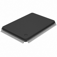
DS21Q43-ATN Maxim Integrated Products, DS21Q43-ATN Datasheet - Page 39

DS21Q43-ATN
Manufacturer Part Number
DS21Q43-ATN
Description
IC FRAMER E1 QUAD 5V 128-TQFP
Manufacturer
Maxim Integrated Products
Datasheet
1.DS21Q43AT.pdf
(60 pages)
Specifications of DS21Q43-ATN
Controller Type
E1 Framer
Interface
Parallel/Serial
Voltage - Supply
4.5 V ~ 5.5 V
Current - Supply
32mA
Operating Temperature
-40°C ~ 85°C
Mounting Type
Surface Mount
Package / Case
128-TQFP, 128-VQFP
Lead Free Status / RoHS Status
Contains lead / RoHS non-compliant
Available stocks
Company
Part Number
Manufacturer
Quantity
Price
Company:
Part Number:
DS21Q43-ATN
Manufacturer:
Maxim Integrated
Quantity:
10 000
9.0 CLOCK BLOCKING REGISTERS
The Receive Channel Blocking Register (RCBR1/ RCBR2/RCBR3/RCBR4) and the Transmit Channel
Blocking Registers (TCBR1/TCBR2/TCBR3/TCBR4) control the RCHBLK and TCHBLK pins
respectively. The RCHBLK and TCHCLK pins are user programmable outputs that can be forced either
high or low during individual channels. These outputs can be used to block clocks to a USART or LAPD
controller in ISDN-PRI applications. When the appropriate bits are set to a 1, the RCHBLK and
TCHCLK pins will be held high during the entire corresponding channel time. See the timing in Section
11 for an example. The TCBRs have alternate mode of use. Via the CCR3.6 bit, the user has the option to
use the TCBRs to determine on a channel-by-channel basis which signaling bits are to be inserted via the
TSRs (the corresponding bit in the TCBRs=1) and which are to be sourced from the TSER pin (the
corresponding bit in the TCBR=0). See the Transmit Data Flow diagram in Section 11 for more details.
RCBR1/RCBR2/RCBR3/RCBR4: RECEIVE CHANNEL BLOCKING
REGISTERS (Address=2B to 2E Hex)
TCBR1/TCBR2/TCBR3/TCBR4: TRANSMIT CHANNEL BLOCKING
REGISTERS (Address=22 to 25 Hex)
NOTE:
If CCR3.6=1, then a 0 in the TCBRs implies that signaling data is to be sourced from TSER and a 1
implies that signaling data for that channel is to be sourced from the Transmit Signaling (TS) registers.
See definition below.
(MSB)
(MSB)
CH16
CH24
CH32
CH16
CH24
CH32
CH8
CH8
SYMBOL
SYMBOL
CH32
CH32
CH1
CH1
CH15
CH23
CH31
CH15
CH23
CH31
CH7
CH7
POSITION
POSITION
RCBR4.7
RCBR1.0
TCBR4.7
TCBR1.0
CH14
CH22
CH30
CH14
CH22
CH30
CH6
CH6
NAME AND DESCRIPTION
Receive Channel Blocking Registers.
0=force the RCHBLK pin to remain low during this channel time
1=force the RCHBLK pin high during this channel time
NAME AND DESCRIPTION
Receive Channel Blocking Registers.
0=force the TCHBLK pin to remain low during this channel time
1=force the TCHBLK pin high during this channel time
CH13
CH21
CH29
CH13
CH21
CH29
CH5
CH5
CH12
CH20
CH28
CH12
CH20
CH28
CH4
CH4
39 of 60
CH11
CH19
CH27
CH11
CH19
CH27
CH3
CH3
CH10
CH18
CH26
CH10
CH18
CH26
CH2
CH2
CH17
CH25
CH17
CH25
CH1
CH9
CH1
CH9
(LSB)
(LSB)
RCBR3 (2D)
RCBR1 (2B)
RCBR2 (2C)
RCBR4 (2E)
TCBR1 (22)
TCBR2 (23)
TCBR3 (24)
TCBR4 (25)
DS21Q43A


