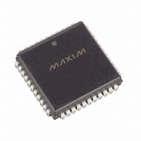
DS2143Q/T&R Maxim Integrated Products, DS2143Q/T&R Datasheet - Page 4

DS2143Q/T&R
Manufacturer Part Number
DS2143Q/T&R
Description
IC CONTROLLER E1 5V LP 44-PLCC
Manufacturer
Maxim Integrated Products
Datasheet
1.DS2143Q.pdf
(44 pages)
Specifications of DS2143Q/T&R
Controller Type
E1 Controller
Interface
Parallel/Serial
Voltage - Supply
4.5 V ~ 5.5 V
Current - Supply
10mA
Operating Temperature
0°C ~ 70°C
Mounting Type
Surface Mount
Package / Case
44-LCC, 44-PLCC
Lead Free Status / RoHS Status
Contains lead / RoHS non-compliant
Available stocks
Company
Part Number
Manufacturer
Quantity
Price
Company:
Part Number:
DS2143Q/T&RDS2143Q/T&R
Manufacturer:
Maxim Integrated
Quantity:
10 000
PIN DESCRIPTION Table 1
6-13
PIN
14
15
16
17
18
19
20
21
22
23
24
25
26
27
28
1
2
3
4
5
SYMBOL
AD0-AD7
WR
RCHCLK
TCHCLK
ALE(AS)
SYSCLK
RSYNC
RLCLK
RD
RLINK
TNEG
RCLK
RNEG
TCLK
TSER
TPOS
RSER
RPOS
BTS
V
CS
(R/
(DS)
SS
W
)
TYPE
I/O
I/O
O
O
O
O
O
O
I
I
I
I
I
I
I
-
I
I
I
Transmit Clock. 2.048 MHz primary clock. A clock must be
applied at the TCLK pin for the parallel port to operate properly.
Transmit Serial Data. Transmit NRZ serial data, sampled on the
falling edge of TCLK.
Transmit Channel Clock. 256 kHz clock which pulses high during
the LSB of each channel. Useful for parallel-to-serial conversion of
channel data. See Section 13 for timing details.
Transmit Bipolar Data. Updated on rising edge of TCLK. For
optical links, can be programmed to output NRZ data.
Address/Data Bus. An 8-bit multiplexed address/data bus.
Bus Type Select. Strap high to select Motorola bus timing; strap
low to select Intel bus timing. This pin controls the function of
assume the function listed in parentheses ().
Read Input (Data Strobe).
Chip Select. Must be low to read or write the port.
Address Latch Enable (Address Strobe). A positive-going edge
serves to demultiplex the bus.
Write Input (Read/Write).
Receive Link Data. Outputs Sa bits. See Section 13 for timing
details.
Signal Ground. 0.0 volts.
Receive Link Clock. 4 kHz to 20 kHz demand clock for the
RLINK output. Controlled by RCR2. See Section 13 for timing
details.
Receive Clock. 2.048 MHz primary clock. A clock must be applied
at the RCLK pin for the parallel port to operate properly.
Receive Channel Clock. 256 kHz clock which pulses high during
the LSB of each channel. Useful for serial to parallel conversion of
channel data. See Section 13 for timing details.
Receive Serial Data. Received NRZ serial data, updated on rising
edges of RCLK.
Receive Sync. An extracted pulse, one RCLK wide, is output at this
pin which identifies either frame (RCR1.6=0) or multiframe
boundaries (RCR1.6=1). If the elastic store is enabled via the
RCR2.1, then this pin can be enabled to be an input via RCR1.5 at
which a frame boundary pulse is applied. See Section 13 for timing
details.
Receive Bipolar Data Inputs. Sampled on falling edge of RCLK.
Tie together to receive NRZ data and disable BPV monitoring
circuitry.
System Clock. 1.544 MHz or 2.048 MHz clock. Only used when
the elastic store function is enabled via the RCR2.1. Should be tied
low in applications that do not use the elastic store.
RD
(DS), ALE(AS), and
4 of 44
WR
DESCRIPTION
(R/
W
) pins. If BTS=1, then these pins
DS2143/DS2143Q


