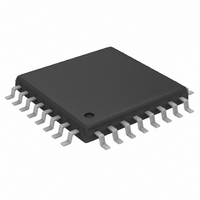
MAX3421EEHJ+T Maxim Integrated Products, MAX3421EEHJ+T Datasheet - Page 18

MAX3421EEHJ+T
Manufacturer Part Number
MAX3421EEHJ+T
Description
IC USB PERIPH/HOST CNTRL 32TQFP
Manufacturer
Maxim Integrated Products
Datasheet
1.MAX3421EETJ.pdf
(32 pages)
Specifications of MAX3421EEHJ+T
Controller Type
USB Peripheral Controller
Interface
USB/Serial
Voltage - Supply
3 V ~ 3.6 V
Current - Supply
15mA
Operating Temperature
-40°C ~ 85°C
Mounting Type
Surface Mount
Package / Case
32-TQFP, 32-VQFP
For Use With
MAX3421EVKIT-1+ - EVAL KIT FOR MAX3421E
Lead Free Status / RoHS Status
Lead free / RoHS Compliant
USB Peripheral/Host Controller
with SPI Interface
The SPI master controls the GPOUT3–GPOUT0 states
by writing to bit 3 through bit 0 of the IOPINS1 (R20)
register. GPOUT7–GPOUT4 states are controlled by
writing to bit 3 through bit 0 of the IOPINS2 (R21) regis-
ter. GPOUT7–GPOUT0 logic levels are referenced to
the voltage on V
state of a GPOUT7–GPOUT0 bit returns the state of the
internal register bit, not the actual pin state. This is use-
ful for doing read-modify-write operations to an output
pin (such as blinking an LED), since the load on the
output pin does not affect the register logic state.
GPX is a push-pull output with a 4-way multiplexer that
selects its output signal. The logic level on GPX is refer-
enced to V
GPXA bits of PINCTL (R17) register to select one of five
internal signals as depicted in Table 5.
Table 5. GPX Output State Due to GPXB
and GPXA Bits
*If SEPIRQ = 1.
• OPERATE: This signal goes high when the
• VBUS_DET: VBUS_DET is the VBCOMP comparator
• BUSACT: USB BUS activity signal (active high).
18
MAX3421E is able to operate after a power-up or
RES reset. OPERATE is active when the RES input
is high and the internal power-on-reset (POR) is
not asserted. OPERATE is the default GPX output.
output. This allows the user to directly monitor the
V
This signal is active whenever there is traffic on
the USB bus. The BUSACT signal is set whenever
a SYNC field is detected. BUSACT goes low during
bus reset or after 32-bit times of J-state.
GPXB
BUS
______________________________________________________________________________________
0
0
1
1
status.
L
. The SPI master writes to the GPXB and
GPXA
L
. As shown in Figure 13, reading the
0
1
0
1
OPERATE (Default State)
VBUS_DET
BUSACT/INIRQ*
SOF
GPX PIN OUTPUT
GPOUT7–GPOUT0
GPX
Figure 14. GPX Output in SOF Mode
Figure 13. Behavior of Read and Write Operations on
GPOUT3–GPOUT0
Figure
Half-Duplex (Bottom) Operation
GPOUT
GPOUT
PACKETS
WRITE
READ
USB
GPX
15. MAX3421E SPI Data Pins for Full-Duplex (Top) and
SOF
CONTROLLER
CONTROLLER
~50%
SPI
SPI
FULL-SPEED
TIME FRAME
REGISTER BIT
1ms
FDUPSPI = 0 (DEFAULT)
FDUPSPI = 1
SOF
FULL-SPEED
TIME FRAME
MAX3421E
MAX3421E
1ms
MOSI
MISO
MOSI
MISO
SOF
GPOUT
PIN


