USBN9603-28M/NOPB National Semiconductor, USBN9603-28M/NOPB Datasheet - Page 17
USBN9603-28M/NOPB
Manufacturer Part Number
USBN9603-28M/NOPB
Description
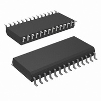
IC CONTROLLER USB 28-SOIC
Manufacturer
National Semiconductor
Datasheet
1.USBN9604-28MNOPB.pdf
(60 pages)
Specifications of USBN9603-28M/NOPB
Controller Type
USB 2.0 Controller
Interface
Parallel/Serial
Voltage - Supply
3 V ~ 5.5 V
Current - Supply
30mA
Operating Temperature
0°C ~ 70°C
Mounting Type
Surface Mount
Package / Case
28-SOIC (7.5mm Width)
Usb Type
Node Controller
Usb Version
1.1
No. Of Ports
2
Supply Voltage Range
3V To 5.5V
Operating Temperature Range
0°C To +70°C
Digital Ic Case Style
SOIC
No. Of Pins
28
Rohs Compliant
Yes
For Use With
USBN9604-HS-EB - KIT NODE CONTROLLER SAMPLE
Lead Free Status / RoHS Status
Lead free / RoHS Compliant
Other names
*USBN9603-28M
*USBN9603-28M/NOPB
USBN9603-28M
*USBN9603-28M/NOPB
USBN9603-28M
Available stocks
Company
Part Number
Manufacturer
Quantity
Price
Company:

Part Number:
USBN9603-28M/NOPB
Manufacturer:
nsc
Quantity:
2 690


4.0 Direct Memory Access (DMA) Support
4.2 AUTOMATIC DMA MODE (ADMA)
The ADMA mode allows the CPU to transfer independently large bulk or isochronous data streams to or from the USB bus.
The application’s DMA controller, together with the ADMA logic, have the capability to split a large amount of data and trans-
fer it in (FIFO size) packets via the USB. In addition, automatic error handling is performed in order to minimize firmware
intervention. The number of transferred data stream bytes must be of a modulo 64 size. The maximum amount of data is
restricted to 256*64 bytes = 16 Kbytes.
To enable an ADMA transfer, the following steps must be performed:
1. The local CPU programs the DMA controller for fly-by demand mode transfers. In this mode, transfers occur only in re-
2. The DMA address counter is programmed to point to the destination memory block in the local shared memory, and the
3. The ADMA enable bit must be set prior to, or at the same time as the DMA enable bit. The DMA enable bit must be
4. The DMA Request Enable bit and DMA Source bits are set in the device.The respective endpoint Enable bit must also
5. The USB host can now perform USB bulk or isochronous data transfers over the USB bus to the receive FIFO or from
See Figures 10 and 11 for the transmit and receive sequences using ADMA mode. See Figures 12 and 13 for the basic
DMA write timing and read timing.
sponse to DMA request via the DRQ pin. The data is read/written from/to the receive/transmit FIFO and written/read in-
to/from local memory during the same bus transaction.
Byte Count register is programmed with the number of bytes in the block to be transferred. The DMA Count register must
be configured with the number of packets to be received or transmitted. If required, the Automatic Error Handling register
must also be configured at this time.
cleared before enabling ADMA mode.
be set.
the transmit FIFO. Steps 5 to 7 of the normal DMA mode are perfromed automatically. The ADMA is stopped either when
the last packet is received or when the DMA Count register has reached the value zero.
Microcontroller
Microcontroller
Set up ADMA
Set up ADMA
Transaction
Figure 10. Transmit Operation Using ADMA Mode
Fill FIFO
Figure 11. Receive Operation Using ADMA Mode
DMA
USB
Transaction
Read FIFO
USB
DMA
Transaction
DMA
Fill FIFO
USB
17
(Continued)
Transaction
Read FIFO
DMA
USB
Last
Transaction
DMA
Last
Read FIFO
USB
time
time
www.national.com
Related parts for USBN9603-28M/NOPB
Image
Part Number
Description
Manufacturer
Datasheet
Request
R

Part Number:
Description:
USB Controller IC
Manufacturer:
National Semiconductor
Datasheet:

Part Number:
Description:
IC CTRLR FULL SPD FUNC 28-SOIC
Manufacturer:
National Semiconductor
Datasheet:

Part Number:
Description:
USBN9603 Universal Serial Bus Full Speed Function Controller with Enhanced DMA Support
Manufacturer:
National Semiconductor
Datasheet:
Part Number:
Description:
Universal Serial Bus Full Speed Node Controller with Enhanced DMA Support
Manufacturer:
National Semiconductor
Part Number:
Description:
USBN9603/USBN9604 Universal Serial Bus Full Speed Node Controller with Enhanced DMA Support
Manufacturer:
National Semiconductor
Datasheet:
Part Number:
Description:
National Semiconductor [8-Bit D/A Converter]
Manufacturer:
National Semiconductor
Datasheet:
Part Number:
Description:
National Semiconductor [Media Coprocessor]
Manufacturer:
National Semiconductor
Datasheet:
Part Number:
Description:
Digitally Controlled Tone and Volume Circuit with Stereo Audio Power Amplifier, Microphone Preamp Stage and National 3D Sound
Manufacturer:
National Semiconductor
Datasheet:
Part Number:
Description:
Digitally Controlled Tone and Volume Circuit with Stereo Audio Power Amplifier, Microphone Preamp Stage and National 3D Sound
Manufacturer:
National Semiconductor
Datasheet:
Part Number:
Description:
AC97 Rev 2 Codec with Sample Rate Conversion and National 3D Sound
Manufacturer:
National Semiconductor
Part Number:
Description:
Manufacturer:
National Semiconductor
Datasheet:
Part Number:
Description:
Manufacturer:
National Semiconductor
Datasheet:
Part Number:
Description:
General Purpose, Low Voltage, Low Power, Rail-to-Rail Output Operational Amplifiers
Manufacturer:
National Semiconductor
Datasheet: