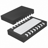
LTC4267CDHC-3#PBF Linear Technology, LTC4267CDHC-3#PBF Datasheet - Page 15

LTC4267CDHC-3#PBF
Manufacturer Part Number
LTC4267CDHC-3#PBF
Description
IC POE 802.3AF W/REG 16-DFN
Manufacturer
Linear Technology
Datasheet
1.LTC4267CGN-3PBF.pdf
(32 pages)
Specifications of LTC4267CDHC-3#PBF
Controller Type
Power over Ethernet Controller (POE)
Interface
IEEE 802.3af
Current - Supply
3mA
Operating Temperature
0°C ~ 70°C
Mounting Type
Surface Mount
Package / Case
16-DFN
Lead Free Status / RoHS Status
Lead free / RoHS Compliant
Voltage - Supply
-
Available stocks
Company
Part Number
Manufacturer
Quantity
Price
temperature exceeds the overtemperature trip point, the
current is reduced to zero and very little power is dissi-
pated in the part until it cools below the overtemperature
set point. Once the LTC4267-3 has charged up the load
capacitor and the PD is powered and running, there will
be minor residual heating due to the DC load current of
the PD fl owing through the internal MOSFET.
During classifi cation, excessive heating of the LTC4267-3
can occur if the PSE violates the 75ms probing time limit.
To protect the LTC4267-3, thermal overload circuitry will
disable classifi cation current if the die temperature exceeds
the overtemperature trip point. When the die cools down
below the trip point, classifi cation current is reenabled.
The PD is designed to operate at a high ambient tem-
perature and with the maximum allowable supply (57V).
However, there is a limit to the size of the load capacitor
that can be charged up before the LTC4267-3 reaches the
overtemperature trip point. Hitting the overtemperature
trip point intermittently does not harm the LTC4267-3,
but it will delay the completion of capacitor charging.
Capacitors up to 200µF can be charged without a problem
APPLICATIO S I FOR ATIO
over the full operating temperature range.
Switching Regulator Main Control Loop
Due to space limitations, the basics of current mode
DC/DC conversion will not be discussed here. The reader
is referred to the detail treatment in Application Note 19
or in texts such as Abraham Pressman’s Switching Power
Supply Design.
In a Power over Ethernet System, the majority of applica-
tions involve an isolated power supply design. This means
that the output power supply does not have any DC elec-
trical path to the PD interface or the switching regulator
primary. The DC isolation is achieved typically through
a transformer in the forward path and an optoisolator in
the feedback path or a third winding in the transformer.
The typical application circuit shown on the front page
of the datasheet represents an isolated design using an
optoisolator. In applications where a nonisolated topology
is desired, the LTC4267-3 features a feedback port and
an internal error amplifi er that can be enabled for this
specifi c application.
U
U
W
U
In the typical application circuit (Figure 11), the isolated
topology employs an external resistive voltage divider
to present a fraction of the output voltage to an external
error amplifi er. The error amplifi er responds by pulling
an analog current through the input LED on an optoiso-
lator. The collector of the optoisolator output presents a
corresponding current into the I
diode. This method generates a feedback voltage on the
I
The voltage on the I
modulator formed by the oscillator, current comparator,
and RS latch. Specifi cally, the voltage at the I
sets the current comparator’s trip threshold. The current
comparator monitors the voltage across a sense resistor
in series with the source terminal of the external N-Chan-
nel MOSFET. The LTC4267-3 turns on the external power
MOSFET when the internal free-running 300kHz oscillator
sets the RS latch. It turns off the MOSFET when the cur-
rent comparator resets the latch or when 80% duty cycle
is reached, whichever happens fi rst. In this way, the peak
current levels through the fl yback transformer’s primary
and secondary are controlled by the I
In applications where a nonisolated topology is desirable
(Figure 11), an external resistive voltage divider can pres-
ent a fraction of the output voltage directly to the V
of the LTC4267-3. The divider must be designed so when
the output is at its desired voltage, the V
will equal the 800mV onboard internal reference. The
internal error amplifi er responds by driving the I
pin. The LTC4267-3 switching regulator performs in a
similar manner as described previously.
Regulator Start-Up/Shutdown
The LTC4267-3 switching regulator has two shutdown
mechanisms to enable and disable operation: an un-
dervoltage lockout on the P
shutdown whenever external circuitry drives the I
pin low. The LTC4267-3 switcher transitions into and out
of shutdown according to the state diagram (Figure 8).
It is important not to confuse the undervoltage lockout
of the PD interface at V
regulator at P
TH
/RUN pin while maintaining isolation.
VCC
. They are independent functions.
TH
/RUN pin controls the pulse-width
PORTN
VCC
with that of the switching
supply pin and a forced
TH
/RUN pin via a series
LTC4267-3
TH
/RUN voltage.
FB
TH
pin voltage
/RUN pin
TH
TH
15
FB
/RUN
/RUN
42673f
pin


