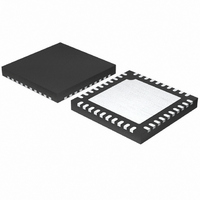
SI3452A-B01-GM Silicon Laboratories Inc, SI3452A-B01-GM Datasheet - Page 16

SI3452A-B01-GM
Manufacturer Part Number
SI3452A-B01-GM
Description
IC POE CONTROLLER MIDSPAN 40QFN
Manufacturer
Silicon Laboratories Inc
Datasheet
1.SI3452B-B01-GM.pdf
(36 pages)
Specifications of SI3452A-B01-GM
Package / Case
40-QFN
Controller Type
Power over Ethernet Controller (POE)
Interface
I²C
Voltage - Supply
3 V ~ 3.6 V
Current - Supply
14mA
Operating Temperature
-40°C ~ 85°C
Mounting Type
Surface Mount
Maximum Power Dissipation
1.2 W
Minimum Operating Temperature
- 40 C
Mounting Style
SMD/SMT
Product
Ethernet Controllers
Standard Supported
IEEE 802.3at, IEEE 802.3af
Supply Voltage (max)
3.6 V
Supply Voltage (min)
3 V
Supply Current (max)
14 mA
Maximum Operating Temperature
+ 85 C
Lead Free Status / RoHS Status
Lead free / RoHS Compliant
Lead Free Status / RoHS Status
Lead free / RoHS Compliant, Lead free / RoHS Compliant
Other names
336-1831-5
Available stocks
Company
Part Number
Manufacturer
Quantity
Price
Company:
Part Number:
SI3452A-B01-GM
Manufacturer:
SILICON
Quantity:
1 001
Company:
Part Number:
SI3452A-B01-GMR
Manufacturer:
SILICON
Quantity:
670
Si3452
4.8.1. Address Pins
Pins with the same name must be externally connected and then tied high or low via a weak (10 k) pull up or pull
down to establish the device address at power up. The Si3452 powers up in either Auto mode or Shutdown mode
depending on the ordering part number. For more information, see "12. Ordering Guide" on page 33.
4.8.2. Address Format
The address byte of the I
AD3, AD2, AD1, and AD0 are the pin-selected address bits (pull up = 1; pull down = 0). For the R/W bit, see
Figure 6. The device will also respond to the global address, 0x30. The Si3452 does not support bus arbitration;
so, a global read command will generally give an invalid result. Global writes can be useful for initialization as well
as for shutting down low-priority ports. Table 16 lists the valid device addresses:
16
Bit 7
2
C communication protocol has the following format:
0
AD3
0
0
0
0
0
0
0
0
1
1
1
1
1
1
1
1
Bit 6
1
Table 15. I
Table 14. Address Pin Assignments
AD2
0
0
0
0
1
1
1
1
0
0
0
0
1
1
1
1
Table 16. Address Selection
Pin #
Bit 5
21
24
25
26
27
28
34
36
0
2
AD1
C Address Byte Protocol
Bit 4
0
0
1
1
0
0
1
1
0
0
1
1
0
0
1
1
AD3
Rev. 1.2
Bit 3
AD0
AD2
0
1
0
1
0
1
0
1
0
1
0
1
0
1
0
1
Pin Name
AD3
AD3
AD2
AD2
AD1
AD0
AD0
AD1
Bit 2
AD1
Address
0x2A
0x2B
0x2C
0x2D
0x2E
0x2F
0x20
0x21
0x24
0x25
0x28
0x29
—
—
—
—
Bit 1
AD0
Valid
N
N
N
N
Bit 0
Y
Y
Y
Y
Y
Y
Y
Y
Y
Y
Y
Y
R/W


