UDT020A0X3-SRZ Lineage Power, UDT020A0X3-SRZ Datasheet - Page 23
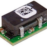
UDT020A0X3-SRZ
Manufacturer Part Number
UDT020A0X3-SRZ
Description
DC/DC Converters & Regulators 3-14.4Vin .6-5.5Vout 20A Neg SMT Digital
Manufacturer
Lineage Power
Datasheet
1.UDT020A0X3-SRZ.pdf
(39 pages)
Specifications of UDT020A0X3-SRZ
Product
Non-Isolated / POL
Input Voltage Range
3 VDC to 14.4 VDC
Input Voltage (nominal)
12 V
Output Voltage (channel 1)
0.6 VDC to 5.5 VDC
Output Current (channel 1)
20 A
Output Voltage
0.6 VDC to 5.5 VDC
Lead Free Status / Rohs Status
Lead free / RoHS Compliant


Preliminary Data Sheet
May 10, 2011
where I
the current measurement, I
current measurement value, T
the inductor winding on the module. Since it may be
difficult to measure T
estimate of the module temperature.
Measuring Output Voltage Using the PMBus
The module can provide output voltage information
using the READ_VOUT command. The command
returns two bytes of data all representing the mantissa
while the exponent is fixed at -10 (decimal).
During manufacture of the module, offset and gain
correction values are written into the non-volatile
memory of the module. The command
VOUT_CAL_OFFSET can be used to read and/or
write the offset (two bytes consisting of a 16-bit
mantissa in two’s complement format) while the
exponent is always fixed at -10 (decimal). The allowed
range for this offset correction is -125 to 124mV. The
command VOUT_CAL_GAIN can be used to read
and/or write the gain correction - two bytes consisting
of a five-bit exponent (fixed at -8) and a 11-bit
mantissa. The range of this correction factor is -0.125
to +0.121, with a resolution of 0.004. The corrected
output voltage reading is then given by:
.
Measuring Input Voltage Using the PMBus
The module can provide output voltage information
using the READ_VIN command. The command returns
two bytes of data in the linear format. The upper five
bits [7:3] of the high data form the two’s complement
representation of the mantissa which is fixed at –5
(decimal). The remaining 11 bits are used for two’s
complement representation of the mantissa, with the
11
valid.
During module manufacture, offset and gain correction
values are written into the non-volatile memory of the
module. The command VIN_CAL_OFFSET can be
used to read and/or write the offset - two bytes
consisting of a five-bit exponent (fixed at -5) and a11-
bit mantissa in two’s complement format. The allowed
range for this offset correction is -2to 1.968V, and the
resolution is 32mV. The command VIN_CAL_GAIN
can be used to read and/or write the gain correction -
two bytes consisting of a five-bit exponent (fixed at -8)
and a 11-bit mantissa. The range of this correction
LINEAGE
V
[
+
V
OUT
VOUT
th
OUT
bit fixed at zero since only positive numbers are
(
,
(
Final
OUT_CORR
Initial
_
POWER
CAL
_
_
Re
is the temperature corrected value of
Re
_
ading
OFFSET
ading
IND
, it may be approximated by an
)
=
)
READ_OUT
×
1 (
IND
+
VOUT
is the temperature of
3 – 14.4Vdc input; 0.45Vdc to 5.5Vdc output; 20A output current
20A Digital Micro DLynx
is the module
_
_
CAL
.
_
GAIN
)]
factor is -0.125 to +0.121, with a resolution of 0.004.
The corrected output voltage reading is then given by:
PMBus
The module supports a number of status information
commands implemented in PMBus. However, not all
features are supported in these commands. A 1 in the
bit position indicates the fault that is flagged.
STATUS_BYTE : Returns one byte of information with
a summary of the most critical device faults.
STATUS_WORD: Returns two bytes of information
with a summary of the module’s fault/warning
conditions.
STATUS_VOUT : Returns one byte of information
relating to the status of the module’s output voltage
related faults.
V
[
+
Reading the Status of the Module using the
V
Position
Position
Position
TM
IN
VIN
IN
Bit
Bit
Bit
(
: Non-isolated DC-DC Power Modules
(
7
6
5
4
3
2
1
0
7
6
5
4
3
2
1
0
7
6
5
4
3
2
1
0
Final
Initial
_
CAL
_
POWER_GOOD# (is negated)
_
Re
CML (Comm. Memory Fault)
CML (Comm. Memory Fault)
_
Re
OFFSET
ading
VOUT fault or warning
IOUT fault or warning
ading
VOUT Overvoltage
VOUT Overvoltage
None of the above
None of the above
IOUT Overcurrent
VIN Undervoltage
IOUT Overcurrent
VIN Undervoltage
Temperature
Temperature
High Byte
Low Byte
)
=
)
Flag
OFF
Flag
OFF
Flag
×
X
X
X
X
X
X
X
1 (
+
VIN
_
CAL
_
Default
Default
Default
GAIN
Value
Value
Value
23
0
0
0
0
0
0
0
0
0
0
0
0
0
0
0
0
0
0
0
0
0
0
0
0
)]
Related parts for UDT020A0X3-SRZ
Image
Part Number
Description
Manufacturer
Datasheet
Request
R

Part Number:
Description:
Manufacturer:
Lineage Power
Datasheet: