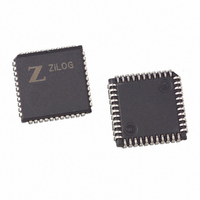
Z8523016VSG Zilog, Z8523016VSG Datasheet - Page 32

Z8523016VSG
Manufacturer Part Number
Z8523016VSG
Description
IC 16MHZ ESCC 44-PLCC
Manufacturer
Zilog
Datasheet
1.Z8523008PSG.pdf
(117 pages)
Specifications of Z8523016VSG
Controller Type
Serial Communications Controller (SCC)
Interface
Bus
Voltage - Supply
4.5 V ~ 5.5 V
Current - Supply
7mA
Operating Temperature
0°C ~ 70°C
Mounting Type
Surface Mount
Package / Case
44-LCC (J-Lead)
Operating Supply Voltage
5 V
Supply Current (max)
9 mA
Maximum Operating Temperature
+ 70 C
Minimum Operating Temperature
0 C
Mounting Style
SMD/SMT
Lead Free Status / RoHS Status
Lead free / RoHS Compliant
Other names
269-3927
Z8523016VSG
Z8523016VSG
Available stocks
Company
Part Number
Manufacturer
Quantity
Price
Company:
Part Number:
Z8523016VSG
Manufacturer:
ZILOG
Quantity:
2 700
Company:
Part Number:
Z8523016VSG
Manufacturer:
ZILOG
Quantity:
2 700
Company:
Part Number:
Z8523016VSG
Manufacturer:
Zilog
Quantity:
231
Part Number:
Z8523016VSG
Manufacturer:
ZILOG
Quantity:
20 000
PS005303-0907
DPLL Counter Tx Clock Source
Read Register 0 Status Latched During Read Cycle
DPLL CLK
synchronous frame is guaranteed to generate two TBE interrupts even if a Reset Transmit
Buffer Interrupt command for the data created interrupt is issued after the CRC interrupt
occurs (Time A in
if the EOM latch resets before the end of the frame.
When the DPLL is selected as the transmit clock source, the DPLL counter output is the
DPLL source clock divided by the appropriate divisor for the programmed data encoding
format. In FM mode (FM0 or FM1), the DPLL counter output signal is the input frequency
divided by 16.
In NRZI mode, the DPLL counter output signal is the input clock cycle divided by 32.
This feature provides a jitter-free output signal that replaces the DPLL transmit clock out-
put as the transmit clock source. This action has no effect on the use of the DPLL as the
receive clock source (see
The contents of Read Register 0, RR0 is latched during a Read operation. The ESCC pre-
vents the contents of RR0 from changing during a Read operation. But, the SCC allows
the status of RR0 to change while reading the register and may require reading RR0 twice.
The contents of RR0 is updated after the rising edge of RD signal.
TxIP Bit
TxBE
Input
Data
Figure
Data
Input Frequency Divided by 16 (FM0 or FM1)
Input Clock Cycle Divided by 32 for NRZI
TxIP 1
Figure 14. DPLL Outputs
Figure 13. TxIP Latching
DPLL Counter
Figure
13). Two
DPLL
CRC1
14).
Reset TBE
CRC2
commands are required. The TxIP latches
DPLL Output to Receiver
DPLL Output to Transmitter
Flag
Time A
TxIP 2
Z80230/Z85230 Enhancements
Product Specification
Z85230/Z80230
27


