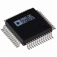
AD1839AAS-REEL Analog Devices Inc, AD1839AAS-REEL Datasheet - Page 20

AD1839AAS-REEL
Manufacturer Part Number
AD1839AAS-REEL
Description
IC CODEC 2ADC/6DAC 24 BIT 52MQFP
Manufacturer
Analog Devices Inc
Type
Stereo Audior
Datasheet
1.AD1839AAS.pdf
(24 pages)
Specifications of AD1839AAS-REEL
Rohs Status
RoHS non-compliant
Data Interface
Serial
Resolution (bits)
24 b
Number Of Adcs / Dacs
2 / 6
Sigma Delta
Yes
S/n Ratio, Adcs / Dacs (db) Typ
105 / 108
Dynamic Range, Adcs / Dacs (db) Typ
105 / 108
Voltage - Supply, Analog
4.5 V ~ 5.5 V
Voltage - Supply, Digital
4.5 V ~ 5.5 V
Operating Temperature
-40°C ~ 85°C
Mounting Type
Surface Mount
Package / Case
52-BQFP
For Use With
EVAL-AD1839AEB - BOARD EVALUATION FOR AD1839A
AD1839A
ADC Control Registers
The AD1839A register map has five registers that are used to
control the functionality and read the status of the ADCs. The
function of the bits in each of these registers is discussed below.
ADC Peak Level
These two registers store the peak ADC result from each
channel when the ADC peak readback function is enabled. The
peak result is stored as a 6-bit number from 0 dB to −63 dB in
1 dB steps. The value contained in the register is reset once it
has been read, allowing for continuous level adjustment as
required. Note that the ADC peak level registers use the six
most significant bits in the register to store the results.
Sample Rate
This bit controls the sample rate of the ADCs. Based on a
24.576 MHz IMCLK, sample rates of 48 kHz and 96 kHz are
available. The MCLK scaling bits in ADC Control 3 should be
programmed appropriately, based on the master clock
frequency.
ADC Power-Down
This bit controls the power-down status of the ADC section and
operates in a manner similar to the DAC power-down.
Table 10. Control Register Map
Register Address
0000
0001
0010
0011
0100
0101
0110
0111
1000
1001
1010
1011
1100
1101
1110
1111
Register Name
DACCTRL1
DACCTRL2
DACVOL1
DACVOL2
DACVOL3
DACVOL4
DACVOL5
DACVOL6
DACVOL7
DACVOL8
ADCPeak0
ADCPeak1
ADCCTRL1
ADCCTRL2
ADCCTRL3
Reserved
Description
DAC Control 1
DAC Control 2
DAC Volume—Left 1
DAC Volume—Right 1
DAC Volume—Left 2
DAC Volume—Right 2
DAC Volume—Left 3
DAC Volume—Right 3
DAC Volume—Left 4
DAC Volume—Right 4
ADC Left Peak
ADC Right Peak
ADC Control 1
ADC Control 2
ADC Control 3
Reserved
Rev. B | Page 20 of 24
High-Pass Filter
The ADC signal path has a digital high-pass filter. Enabling this
filter removes the effect of any dc offset in the analog input
signal from the digital output codes.
ADC Data-Word Width
These two bits set the word width of the ADC data.
ADC Data Format
The AD1839A serial data interface can be configured to be
compatible with a choice of popular interface formats, including
I
Master/Slave Auxiliary Mode
When the AD1839A is operating in the auxiliary mode, the
auxiliary ADC control pins, AUXBCLK and AUXLRCLK, which
connect to the external ADCs, can be set to operate as a master
or slave. If the pins are set in slave mode, one of the external
ADCs should provide the LRCLK and BCLK signals.
ADC Peak Readback
Setting this bit enables ADC peak reading. See the ADCs
section for more information.
2
S, LJ, RJ, or DSP modes.
Type
R/W
R/W
R/W
R/W
R/W
R/W
R/W
R/W
R/W
R/W
R
R
R/W
R/W
R/W
R/W
Width
10
10
10
10
10
10
10
10
10
10
6
6
10
10
10
10
Reset Setting (Hex)
000
000
3FF
3FF
3FF
3FF
3FF
3FF
3FF
3FF
000
000
000
000
000
Reserved


