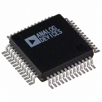
AD1839AAS-REEL Analog Devices Inc, AD1839AAS-REEL Datasheet - Page 12

AD1839AAS-REEL
Manufacturer Part Number
AD1839AAS-REEL
Description
IC CODEC 2ADC/6DAC 24 BIT 52MQFP
Manufacturer
Analog Devices Inc
Type
Stereo Audior
Datasheet
1.AD1839AAS.pdf
(24 pages)
Specifications of AD1839AAS-REEL
Rohs Status
RoHS non-compliant
Data Interface
Serial
Resolution (bits)
24 b
Number Of Adcs / Dacs
2 / 6
Sigma Delta
Yes
S/n Ratio, Adcs / Dacs (db) Typ
105 / 108
Dynamic Range, Adcs / Dacs (db) Typ
105 / 108
Voltage - Supply, Analog
4.5 V ~ 5.5 V
Voltage - Supply, Digital
4.5 V ~ 5.5 V
Operating Temperature
-40°C ~ 85°C
Mounting Type
Surface Mount
Package / Case
52-BQFP
For Use With
EVAL-AD1839AEB - BOARD EVALUATION FOR AD1839A
AD1839A
FUNCTIONAL OVERVIEW
ADCS
There are two ADC channels in the AD1839A, configured as a
stereo pair. Each ADC has fully differential inputs. The ADC
section can operate at a sample rate of up to 96 kHz. The ADCs
include on-board digital decimation filters with 120 dB stop-
band attenuation and linear phase response, operating at an
oversampling ratio of 128 (for 48 kHz operation) or 64 (for
96 kHz operation).
The peak level information for each ADC may be read from the
ADC Peak 0 and ADC Peak 1 registers. The data is supplied as a
6-bit word with a maximum range of 0 dB to −63 dB and a
resolution of 1 dB. The registers hold peak information until
read; after reading, the registers are reset so that new peak
information can be acquired. (Refer to the register description
in Table 10 for details of the format.) The two ADC channels
have a common serial bit clock and a left-right framing clock.
The clock signals are all synchronous with the sample rate.
The ADC digital pins, ABCLK and ALRCLK, can be set to
operate as inputs or outputs by connecting the M /S pin to
ODVDD or DGND, respectively. When the pins are set as
outputs, the AD1839A generates the timing signals. When the
pins are set as inputs, the timing must be generated by the
external audio controller.
DACS
The AD1839A has six DAC channels arranged as three
independent stereo pairs, with six single-ended analog outputs.
Each channel has its own independently programmable
attenuator, adjustable in 1,024 linear steps. Digital inputs are
supplied through three serial data input pins (one for each
stereo pair) and a common frame (DLRCLK) and bit clock
(DBCLK). Alternatively, one of the packed data modes can be
used to access all six channels on a single TDM data pin. A
stereo replicate feature is included where the DAC data sent to
the first DAC pair is also sent to the other DACs in the part.
The AD1839A can accept DAC data at a sample rate of 192 kHz
on DAC 1 only. The stereo replicate feature can then be used to
copy the audio data to the other DACs.
Each of the output pins sits at a dc level of V
±1.4 V for a 0 dB digital input signal. A single op amp, third-
order, external low-pass filter is recommended to remove high
frequency noise present on the output pins. Note that the use of
op amps with low slew rate or low bandwidth may cause high
frequency noise and tones to fold down into the audio band;
care should be exercised in selecting these components.
The FILTD pin should be connected to an external grounded
capacitor. This pin reduces the noise of the internal DAC bias
circuitry, thus reducing the DAC output noise. At times, this
capacitor may be eliminated with little effect on performance.
REF
and swings
Rev. B | Page 12 of 24
DAC AND ADC CODING
The DAC and ADC output data stream is in a twos complement
encoded format. A 16-bit, 20-bit, or 24-bit word width can be
selected. The coding scheme is detailed in Table 6.
Table 6. Coding Scheme
Code
01111......1111
00000......0000
10000......0000
AD1839A CLOCKING SCHEME
By default, the AD1839A requires an MCLK signal that is
256 times the required sample frequency up to a maximum of
12.288 MHz. The AD1839A uses a clock scaler to double the
clock frequency for use internally. The default setting of the
clock scaler is Multiply by 2. The clock scaler can also be set to
Multiply by 1 (bypass) or Multiply by 2/3. The clock scaler is
controlled by programming the bits in the ADC Control 3
register. The internal MCLK signal, IMCLK, should not exceed
24.576 MHz to ensure correct operation.
The MCLK of the AD1839A should remain constant during
normal operation of the DAC and ADC. If it is required to
change the MCLK rate, the AD1838A should be reset. Also, if
MCLK scaler needs to be modified so that the IMCLK does not
exceed 24.576 MHz, this should be done during the internal
reset phase of the AD1839A by programming the bits in the
first 3,072 MCLK periods following the reset.
Selecting the DAC Sampling Rate
The AD1839A DAC engine has a programmable interpolator
that allows the user to select different interpolation rates based
on the required sample rate and MCLK value available. Table 7
shows the settings required for sample rates based on a fixed
MCLK of 12.288 MHz.
Table 7. DAC Sample Rate Settings
Sample Rate
48 kHz
96 kHz
192 kHz
Selecting an ADC Sample Rate
The AD1839A ADC engine has a programmable decimator that
allows the user to select the sample rate based on the MCLK
value. By default, the output sample rate is IMCLK/512. To
achieve a sample rate of IMCLK/256, the sample rate bit in the
ADC Control 1 register should be set as shown in Table 8.
Table 8. ADC Sample Rate Settings
Sample Rate
IMCLK/512
IMCLK/256
Interpolator Rate
8×
4×
2×
ADC Control 1 Register
1100000xx0xxxxxx (48 kHz)
1100000xx1xxxxxx (96 kHz)
Level
+FS
0 (Ref level)
−FS
DAC Control 1 Register
000000xxxxxxxx00
000000xxxxxxxx01
000000xxxxxxxx10


