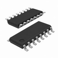
SI3000-KS Silicon Laboratories Inc, SI3000-KS Datasheet - Page 18

SI3000-KS
Manufacturer Part Number
SI3000-KS
Description
IC VOICE CODEC 3.3V/5V 16SOIC
Manufacturer
Silicon Laboratories Inc
Type
Voice-Band Codecr
Specifications of SI3000-KS
Package / Case
16-SOIC (0.154", 3.90mm Width)
Data Interface
Serial
Resolution (bits)
16 b
Number Of Adcs / Dacs
1 / 1
Sigma Delta
No
Dynamic Range, Adcs / Dacs (db) Typ
84 / 84
Voltage - Supply, Analog
3 V ~ 5.25 V
Voltage - Supply, Digital
3 V ~ 5.25 V
Operating Temperature
0°C ~ 70°C
Mounting Type
Surface Mount
Number Of Adc Inputs
3
Number Of Dac Outputs
2
Conversion Rate
12 KSPs
Interface Type
Serial
Resolution
16 bit
Maximum Operating Temperature
+ 70 C
Mounting Style
SMD/SMT
Minimum Operating Temperature
0 C
Number Of Channels
1 ADC, 1 DAC
Lead Free Status / RoHS Status
Contains lead / RoHS non-compliant
Lead Free Status / RoHS Status
Lead free / RoHS Compliant, Contains lead / RoHS non-compliant
Available stocks
Company
Part Number
Manufacturer
Quantity
Price
Part Number:
SI3000-KS
Manufacturer:
SILICONLABS/芯科
Quantity:
20 000
S i3 00 0
PLL Lock Times
The Si3000 changes sample rates very quickly.
However, lock time will vary based on the programming
of the clock generator. The following relationship
describes the boundaries on PLL locking time:
It is recommended that the PLL be programmed during
initialization.
18
PLL lock time < 1 ms
Table 12. MCLK Examples for 8 kHz
MCLK (MHz)
10.0800
10.5600
14.7456
16.0000
18.4320
24.5760
25.8048
33.7600
44.2368
46.0800
47.9232
48.0000
56.0000
11.0592
1.8432
4.0000
4.0960
5.2800
5.7600
6.1440
8.1920
9.2160
12.288
59.200
175
185
211
117
N1
25
33
63
33
27
25
63
27
75
9
1
9
3
1
9
3
9
9
3
9
200
256
256
256
128
100
100
256
100
128
128
M1
10
64
20
40
10
25
64
20
25
64
5
5
8
Rev. 1.1
The final design consideration for the clock generator is
the update rate of PLL. The following criteria must be
satisfied in order for the PLL to remain stable:
Where F
Setting Generic Sample Rates
The above clock generation description focuses on
common modem sample rates. The restrictions and
equations above still apply; however, a more generic
relationship between MCLK and Fs (the desired sample
rate) is needed. The following equation describes this
relationship:
where Fs is the sample frequency, and all other symbols
are shown in Figure 18.
Knowing the MCLK frequency and desired sample rate
the values for the M1 and N1 registers can be
determined. When determining these values, remember
to consider the range for each register as well as the
minimum update rate for the first PLL.
The values determined for M1 and N1 must be adjusted
by minus one when determining the value written to the
respective registers. This is due to internal logic, which
adds one to the value stored in the register. This
addition allows the user to write a zero value in any of
the registers and the effective divide-by is one. A
special case occurs when both M1 and N1 are
programmed with a zero value. When M1 and N1 are
both zero, the PLL is bypassed.
Sleep Mode
The Si3000 supports a low-power sleep mode. Sleep
mode is activated by setting the Chip Power Down
(CPD) bit in register 1. When the Si3000 is in sleep
mode, the MCLK signal may be stopped or remain
active, but it must be active before waking up the
Si3000. To take the Si3000 out of sleep mode, pulse the
reset pin (RESET) low. In summary, the power down/up
sequence is as follows:
1. Set the Power Down bit (PDN, register 6, bit 3).
2. MCLK may stay active or stop.
3. Restore MCLK before initiating the power up sequence.
4. Reset the Si3000 using the RESET pin (after MCLK is
5. Program the registers to desired settings.
present).
UP1
F
is shown in Figure 18.
UP1
=
M1
------- -
N1
F
MCLK
=
5 1024 Fs
------------------------------- -
MCLK
N1
144kHz


