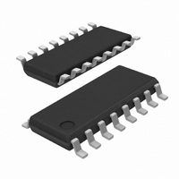
SI3000-KS Silicon Laboratories Inc, SI3000-KS Datasheet - Page 17

SI3000-KS
Manufacturer Part Number
SI3000-KS
Description
IC VOICE CODEC 3.3V/5V 16SOIC
Manufacturer
Silicon Laboratories Inc
Type
Voice-Band Codecr
Specifications of SI3000-KS
Package / Case
16-SOIC (0.154", 3.90mm Width)
Data Interface
Serial
Resolution (bits)
16 b
Number Of Adcs / Dacs
1 / 1
Sigma Delta
No
Dynamic Range, Adcs / Dacs (db) Typ
84 / 84
Voltage - Supply, Analog
3 V ~ 5.25 V
Voltage - Supply, Digital
3 V ~ 5.25 V
Operating Temperature
0°C ~ 70°C
Mounting Type
Surface Mount
Number Of Adc Inputs
3
Number Of Dac Outputs
2
Conversion Rate
12 KSPs
Interface Type
Serial
Resolution
16 bit
Maximum Operating Temperature
+ 70 C
Mounting Style
SMD/SMT
Minimum Operating Temperature
0 C
Number Of Channels
1 ADC, 1 DAC
Lead Free Status / RoHS Status
Contains lead / RoHS non-compliant
Lead Free Status / RoHS Status
Lead free / RoHS Compliant, Contains lead / RoHS non-compliant
Available stocks
Company
Part Number
Manufacturer
Quantity
Price
Part Number:
SI3000-KS
Manufacturer:
SILICONLABS/芯科
Quantity:
20 000
Clock Generation Subsystem
The Si3000 contains an on-chip clock generator. Using
a single MCLK input frequency, the Si3000 can
generate all the desired standard modem sample rates,
as well as the common 11.025 kHz rate for audio
playback.
The clock generator consists of a phase-locked loop
(PLL1) that achieves the desired sample frequency.
Figure 18
architecture of the PLL allows for fast lock time on initial
start-up, fast lock time when changing modem sample
rates and high noise immunity. A large number of MCLK
frequencies between 1 MHz and 60 MHz are supported.
Programming the Clock Generator
As noted in Figure 18, the clock generator must output a
clock equal to 1024*Fs, where Fs is the desired sample
illustrates
FSYNC
(mode 1)
FSYNC
(mode 0)
SDI
SDO
MCLK
the
Figure 17. Secondary Frame Format—Read Cycle
High Z
8 bits
Figure 18. Clock Generation Subsystem (PLL)
N1
clock
P
D
F
D15 D14 D13 D12 D11 D10 D9
generator.
UP1
0
8 bits
0
M1
R/W
1
A
VCO1
The
A
Rev. 1.1
A
rate. The 1024*Fs clock is determined through
programming of the following registers:
N1 (register 3) and M1 (register 4) are 8-bit unsigned
values. F
Table 12 list several standard crystal rates that could be
supplied to MCLK.
When programming the registers of the clock generator,
the order of register writes is important. For PLL
updates, N1 (register 3) must always be written first,
immediately followed by a write to M1 (register 4).
Note: The values shown in Table 12 satisfy the equations
A
D8
Register 3 - N1 divider, 8 bits.
Register 4 - M1 divider, 8 bits
A
*Note: See PLL bit in Register 2
F
D7
D7
above. However, when programming the registers for
N1 and M1, the value placed in these registers must be
one less than the value calculated from the equations.
D
5 or
10 *
PLL1
MCLK
D6
D
D5 D4 D3 D2
D
is the clock provided to the MCLK pin.
D
1024
D
•
D
fs
D1 D0
D
D0
D
High Z
Si3000
17


